


We often face problem while reading the values of ICs and miniature SMD components, detecting cracks or shorts in tracks in a PCB, or reading a finely-graduated vernier scale. Here is a solution to the problem in the form of a simple optical magnifier that simultaneously magnifies and illuminates the object.
Circuit and working of Illuminated Optical Magnifier
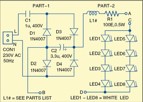
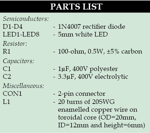
The main constituents of the magnifier are a convex lens with focal length of about 10cm for magnification of the object, a set of eight white LEDs to illuminate the object, an LED driver circuit for powering the LEDs and some other components. Fig. 1 shows the circuit diagram of the optical magnifier.
Download PCB and Component layout PDFs: click here
Snubber capacitor C1 at the input reduces the line-input voltage of 230V to a very-low-level AC voltage. The full-wave bridge rectifier, comprising diodes D1 through D4, converts the low-level AC voltage into DC voltage. C2 is a smoothening capacitor. Series current-limiting resistor R1 and series inductor coil L1 avoid voltage spikes.

Two branches of the LEDs are connected in parallel. Each branch has four LEDs connected in series as shown in Fig. 1.
Construction and testing
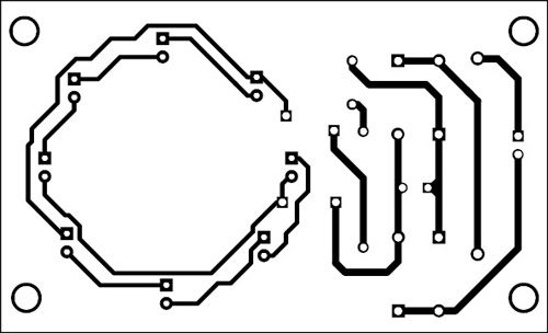
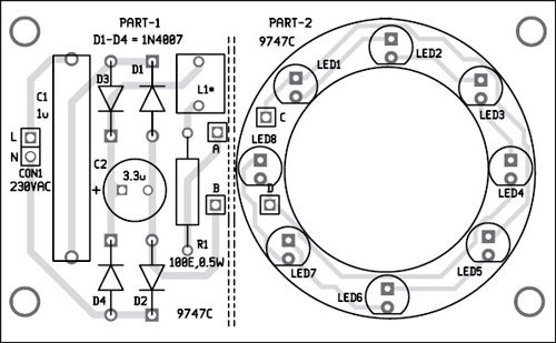
A single-side PCB for the optical magnifier is shown in Fig. 2 and its component layout in Fig. 3. Before assembling the circuit, cut the PCB across the dotted line and assemble the circuit on two separate PCBs as part 1 and part 2.

The PCB for mounting the LEDs (part 2) is in annular shape as shown in Fig. 3. LEDs are placed around the lens as shown in Fig. 4. Drill eight holes to house LED holders. You can also have a press-fit arrangement.
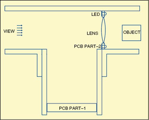
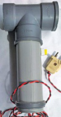
Enclose PCB part 2 in the PVC pipe in such a way that light from the LEDs falls on the object but the LEDs do not obstruct the view. Enclose PCB part 1 in the side tube. Power PCB part 1 by connecting it to the mains by a flexible power cord. Ensure proper wiring insulation to avoid shock while using the magnifier.
Fit PCB part 1 that has the circuit for powering the LEDs in the side tube as shown in Fig. 4. Outer diameter of PCB part 1 will be the same as the inner diameter of the side tube. Connect points A and B on part 1 to points C and D on part 2, respectively, through external wires.
The arrangement shown in Fig. 4 is schematic and not to scale. The outer diameter of the lens will decide the overall arrangement. You will have to make suitable clamps to hold the lens and PCBs inside the tube. The prototype used by the author is shown in Fig. 5.
Millind M. Sutar is assistant professor of Physics at S.M. Dr Bapuji Salunkhe College, Miraj, Dist. Sangli, Maharashtra.

This is a very good project can you please add a camera and a display to this project .I wish to learn using camera and display in circuits. Any guidance Please
Job well done but pls calculation for values use.
If it is used 9 V battery would be more safe and handy .