


Presented here is a USB data acquisition system that can be used to interface six sensors and four digital-to-analogue channels. The acquired voltage levels can be displayed on a personal computer (PC). The DAQ device may be calibrated for precision and benchmarked with various standards, and delivered as an inexpensive USB DAQ product for hobbyists and students.
Irrespective of our stream of engineering or science, most of us do programming and data analysis on computers due to ease in data handling, storage and manipulation.
This project may be helpful for those who want to develop an integrated system that consists of a DAQ and other system circuitry in a single unit. It would provide a greater insight to the design and development of a USB DAQ system itself! The article includes details of circuit designs, software development for user-interface using C# and LabView, printed circuit board (PCB) development and test results.

It is assumed that the reader is familiar with basic ‘C’ programming and AVR programming styles. However, best efforts have been made to make the contents logical enough to help even a beginner understand the project and tweak with the codes.

DAQ systems
 A DAQ system acquires data from a sensor mounted on a physical system and brings it to your PC.
Typically, the output from a sensor is available in the form of a voltage signal. For example, the output from a commonly used temperature sensor like LM35 is 10mV/°C under normal environmental conditions, which varies linearly with temperature. Hence you can calibrate the measured voltage to the temperature of the surroundings it is being interfaced with. Same is the case with a pressure sensor, LVDT, etc.
You may also need to trigger a device from a PC with a voltage signal, or you may require a dynamically changing voltage level to drive a certain drive system, e.g., a linear servo motor. You may also require to count an event which is signaled by a voltage pulse, such as in flywheel counters or robotic shaft encoders.
Most of the commercially available DAQ systems come with all the above-mentioned features of counters, analogue inputs and outputs, digital inputs and outputs, etc. However, these systems are quite expensive and come with a paid driver for interfacing. Most of them can only be used with the proprietary software of the manufacturer.
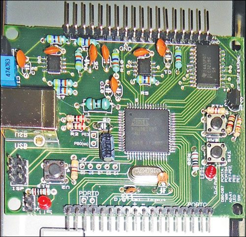
This project is intended for those who want to make their own system for data acquisition due to the limitation of their total project cost or installation where one cannot use commercially available DAQ (such as in a nuclear or defense installation). The author’s prototype is shown in Fig. 1.
Circuit and working
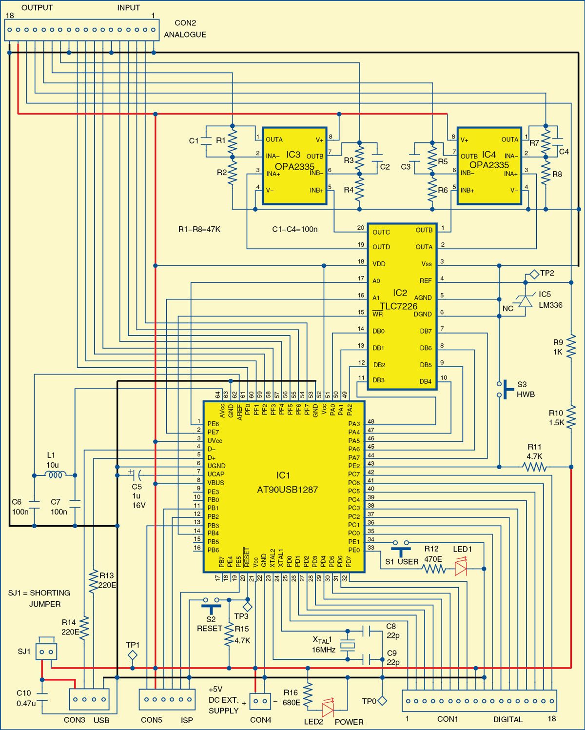
Fig. 2 shows the circuit of USB data acquisition system.
 AT90USB1287
 AT90USB1287
The heart of the system is a 64-pin ATMEL USB chip AT90USB1287, which is an 8-bit microcontroller that can do USB communication and take analogue input through its eight 10-bit analogue-to-digital converters (ADCs). It has 48 programmable input/output pins. The microcontroller runs on a 16MHz clock and has 128 kB of flash memory. As the microcontroller does not have any digital-to-analogue converter (DAC) on its output pins, we required an external chip for this purpose. We used TLC7226 from Texas Instruments (TI), which is an 8-bit DAC with quad outputs.
Before finalising the design, ensure that all the AVR hardware design considerations mentioned in ATMEL application note are met. You can easily get IC samples for academic and research purposes, which the manufacturers always support.
TLC7226
This is a 20-pin dual-in-line chip. You may refer to its datasheet from TI for more details. This IC is driven by a reference diode LM336 to have a regulated voltage supply of 2.5V. So for an input ranging from 0 to 255 through parallel eight pins of the microcontroller, the output varies from 0 to 2.5V. As the output desired is 5V, we have used a voltage amplifier with gain set at ‘2.’ For voltage amplification we used quad op-amp OPA2335 from Texas Instruments, which has zero drift and low offset voltage of 5 μV.
Power supply
The circuit is powered from the USB port, which provides a voltage output of up to 4.5V. If you need to connect the output pins to a load larger than that supported by your USB port (typically 500 mA per port), use an external power source of 5V and remove the USB power jumper (SJ1) shown in Fig. 6.
Connectors
Since the system requires interfacing with an external device for input and output, we have used connectors for various purposes. One 18-pin connector (CON2) is used for analogue inputs and outputs, while another 18-pin connector (CON1) is used for digital inputs and outputs. There is also a 6-pin connector for ISP interfacing and a 2-pin shorting jumper connector for power supply from the USB port.
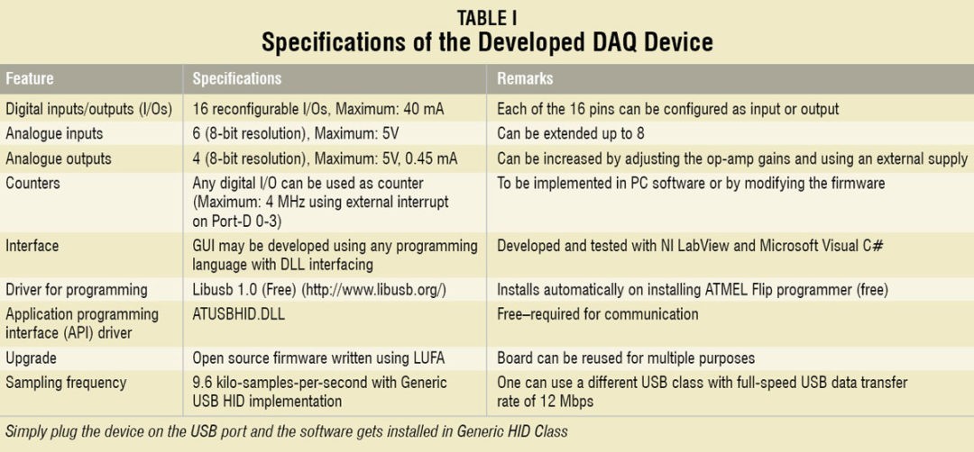
Specifications of the developed DAQ device are listed in Table I.
Construction
Once done with the schematic of the project, you need to mount the components on the provided PCB. An actual-size, double-side, solder-side PCB track layout of USB data acquisition system is shown in Fig. 3 and component-side track layout in Fig. 4. The component layout is shown in Fig. 5. The author’s assembled board with input and output pin details is shown in Fig. 6.
The original board routing and layout design was done by the author on a four-layered board with inner layers supplying the power. Having continuous copper layers in the inner layers provided better stability to ADC and DAC systems.
The board was built with a mix of surface-mount device (SMD) and through-hole technology (THT) components as we could not obtain small quantities of the discrete components in SMD packages. You can choose to use only SMD components to have a compact design. You can also try assembling the circuit on a double-layered board to cut down the development cost.
Firmware and software design
The firmware was developed using open source library ‘Lightweight USB Framework for AVR,’ commonly known as LUFA. It requires free compiler WinAVR GCC 2010 to be installed in your PC. It is advised to install AVR Studio 4 before WinAVR as programming and compilation are easier in AVR Studio. Now load project file GenericHID.aps file (from www.efymag.com or EFY DVD of this month’s EFY Plus) into AVR Studio environment. Compile the code to generate the hex code.
Burning the hex code. Microcontroller AT90USB1287 comes with a preloaded bootloader program that can be used to burn a hex file through USB using ATMEL Flip software.


Download PCB and Component Layout PDFs: Click here
Download Source Code: Click here
Press S3 (HWB) button and S2 reset button simultaneously and then first release S2 while S3 is pressed. This will put the board into an inbuilt bootloader programming mode. In programming mode, the board can be seen in device manager of the PC. You can load the hex code into the MCU using ATMEL Flip programmer.
But to make a generic code run with read and write support in flash memory, you need to erase the entire flash (default bootloader) and load a new bootloader called ‘ATMEL USB DFU Bootloader’ from ATMEL’s website. This also enables the microcontroller to run at its full speed of 16 MHz. You just need to make necessary changes in the fuses to make it run with external clock of 16 MHz (without CKDIV8 fuse enabled). Now burn the new bootloader using any ISP programmer by connecting the programmer to the ISP connector on the board.
User-interface program
After assembling the components on the PCB, you need to interface the board with the PC for data exchange. For that, you have software that communicates with the physical hardware through USB interface using its device driver dynamic link library (DLL). The graphical-user-interface (GUI) software was developed using Microsoft Visual C# 2010.net and NI LabView Version 8.6 (2008).
The hardware developed has the firmware loaded onto the flash memory of the microcontroller on the DAQ board. To design the GUI program, first you need to know how the firmware in the board and the PC should communicate.
The firmware continuously sends and receives eight bytes of data to and from the PC. Ports C and D of the microcontroller are connected to CON1 digital I/O pins. The first two bytes from the PC contain data for data direction registers (DDRs), namely, DDRC and DDRD. The next two consecutive bytes, i.e., the third and the fourth bytes, contain the value that is to be written to each port. Each bit in the register DDRx and PORTx values corresponds to a physical pin of the microcontroller’s ports C and D. For example, to set the fourth and sixth pins as outputs, you need to write to the DDRx register a value equivalent to the binary value ‘00101000.’ To set the fourth pin ‘high’ you need to write to the corresponding PORTx register a value of ‘00001000.’ Writing ‘1’ at any other place in the PORTx register will enable the pull-up at the corresponding physical pin. The pins are input pins by default.
The remaining four bytes are the values for DAC outputs. These are transferred to TLC7226’s parallel input pins via port A of the microcontroller. To write a value to the DAC output, select the DAC output by A0 (pin 17) and A1 (pin 16) of the chip TLC7226, make the selected pin active by lowering WR pin (pin 15) of the chip, write the value to data pins of TLC7226 (DB0 through DB7) and finally make WR pin high before exiting the write subroutine.
The firmware sends in the first six bytes data collected from the analogue input pins of the microcontroller. The remaining two bytes sent by it contain the pin status of 8-bit wide port C and port D, respectively.
If you are not using the digital input pins, the firmware can be modified to read all the available eight analogue inputs of the microcontroller. By receiving and sending ten bytes, the code can be extended to use all the analogue inputs without disturbing the digital inputs. However, this reduces the sampling speed.
All the analogue inputs are sampled one by one and copied to the send buffer. It is advised to connect the unused analogue inputs to ground, to make the sampling stable. You are requested to go through the files board.c and GenericHID.c in LUFA101122\Demos\Device\LowLevel\GenericHID folder of the project for extensive reference. The codes are well remarked for future modifications. All the relevant source codes are included in this month’s EFY DVD.
As the microcontroller has its own timers, the code can be extended to have a fixed sampling speed for any real-time application. Filters can also be implemented in the firmware itself for noiseless sensing.
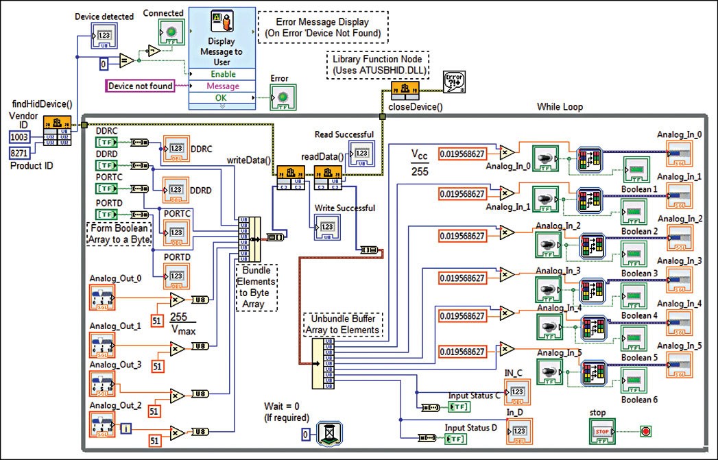
The software implements the ATMEL application note on USB generic human interface device (HID). It uses functions findHidDevice, readData, writeData and closeDevice defined in ATUSBHID.DLL. As shown in the GUI screenshot, the software connects to the DAQ board through USB vendor ID for ATMEL (03EB in hexadecimal) and product ID for the microcontroller (204F in hexadecimal).
An 8-byte send-buffer is prepared based on the settings of digital input/output selections, their corresponding values and analogue output values. This is sent continuously through a timer event in C# routine, within an infinite loop in LabView scheme.
Similarly, the incoming eight bytes are read to obtain the six 8-bit analogue input values corresponding to the voltage available at ADC pins and two 8-bit values for the input pin status. The graphical user interface (GUI) shows the various ADC inputs and DAC outputs.
Fig. 7 shows the front-end GUI screenshot of C# program output. Fig. 8 shows the block diagram for LabView VI, which generates a GUI analogous to that generated by the C# program. Additionally, it explores the digital input and output capability as well. LabView being a block-diagram-based programming language, it explains the functional implementation of the software very clearly. A 30-day evaluation version of the latest LabView version can be freely downloaded from the Internet.
The C# program and the LabView VI are used only to demonstrate the correct functioning of the board. On similar lines, you can develop your own code in various other programming languages. (Note that LabView was not tested at EFY Lab.)
Testing and test results
Before getting started, using a multimeter you need to measure the USB voltage that your system is supplying. Save this value in the parameter V_Max_USB of the program.
The developed prototype was tested with various sensors like potentiometer, LDR and analogue accelerometer. The sensed ADC output shown by the software was found to be closely matching with the physical measurements.
Similarly, the DAC outputs were tested physically using a digital multimeter and found to be in agreement with the desired voltage values set in the software. Maximum variation from the actual value was found to be within ±0.02V. Apart from the ADC and DAC tests, the digital inputs and outputs were found to be responding properly to the software. Figs 9 and 10 show the plots for the ADC and DAC tests, respectively.
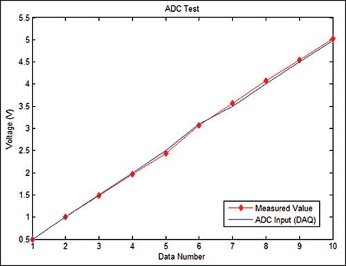
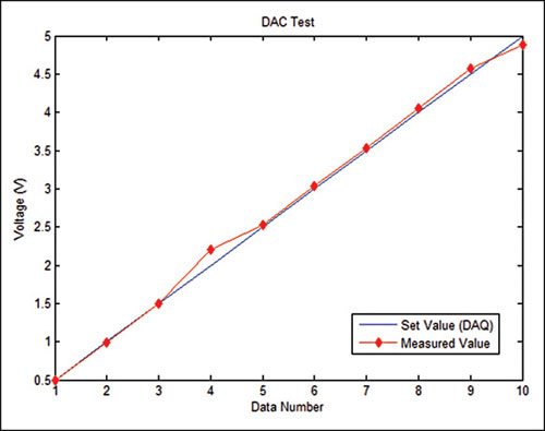
With Generic HID mode of USB communication, the device runs at 9.6 kilo-samples per second, which is good enough to handle a situation where the inputs and outputs are dynamically varying. Though the developed DAQ device is quite basic compared to the existing technology, it can be very helpful for everyday use where one needs an inexpensive device with reasonably good reliability and precision. It has the potential to replace advanced DAQ devices like NI USB 6008/6009 (which it closely resembles to) in smaller enterprises that don’t have much stringent demands and certification requirements.
Troubleshooting
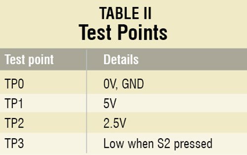
If the software on your PC doesn’t respond, first check the circuit for proper connections. You can also try closing the application and restarting it. If the problem persists, check voltages at various test points as per Table II.
The author has uploaded on YouTube videos of this DAQ device being tested using C# and LabView interface. You may watch the same for better understanding.
Further application
The board can be reprogrammed for different purposes with different customised programs for the connected I/Os.


Can it Work with MATLAB
PS Note: i am a chemical engineering student
Yes, you can interface with MATLAB also
cost for this circuit making
Can I get the youtube link of this project?
i want digital out 100ma current how can i get?
Seem to me source code link is broken?
Hi! Where’s the code?? The link for code downloads pdf’s with pcb’s. Thank you
Thank you for your comment, we have updated the article with the correct link.
what is the maximum input frequency i can get