Presented here is a digital clock that also functions as a rechargeable light lantern and a mobile charger. The digital clock has all the basic functions like date-time display, alarm and room temperature display. It is powered by a lead-acid battery, which can be recharged through solar power or mains power supply. So the clock never runs out of power.
The digital clock is provided with a female USB socket, which can be used to charge most of your mobile phones and gadgets. Its dedicated battery charging and load cut-off circuitry takes care of the battery through exact charging topology and prevents it from getting over-charged or under-charged.
Block diagrams
The functional unit of the digital clock is divided into power unit and main clock unit. Block diagram of the power unit is shown in Fig. 1.

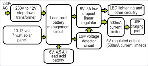
The power unit provides continuous power to the digital clock and other circuits. Its lead-acid battery can be charged through solar power or AC mains power. The battery management circuit is designed to accept power from two sources at the same time but gives priority to the mains power. So if the solar power is low or unavailable, users can plug the battery into the AC mains wall supply to charge it.
A solar photovoltaic panel is used to directly convert solar light and heat energy into electricity. To harness AC mains power for the circuit, a step-down transformer is used. It converts high-voltage AC into low-voltage AC. This AC voltage is rectified and converted into DC, and then further smoothened by using capacitors as low-pass filters. After this, the power becomes acceptable for the battery management circuit.

The lead-acid battery is directly connected to the battery management circuit, which takes care of battery charging with charging voltage and current maintained to acceptable limits. This ensures longer battery life, capacity and optimal usage.
Next, a comparator circuit is used. It checks the battery voltage against its internal reference voltage and shuts off the load, thus preventing the battery from further discharging. A linear low-dropout (LDO) voltage regulator is used to derive regulated 5V from the battery rail. This 5V rail is non-current-limited and powers most of the circuitry ahead, including LEDs. A current-limited load switch is used to derive 5V rail, which is current-limited to 500mA for USB charging applications in order to prevent USB application from immediately discharging the clock battery.
Block diagram of the main clock unit is shown in Fig. 2. The microcontroller in the circuit keeps track of all the sensors and switches connected to it, makes decisions and calculations, and finally updates the display section. In this section, the non-current-limited 5V rail from the power section is converted into 3.3V rail via a 3.3V LDO voltage regulator (UCC383) that powers the microcontroller and other peripherals.
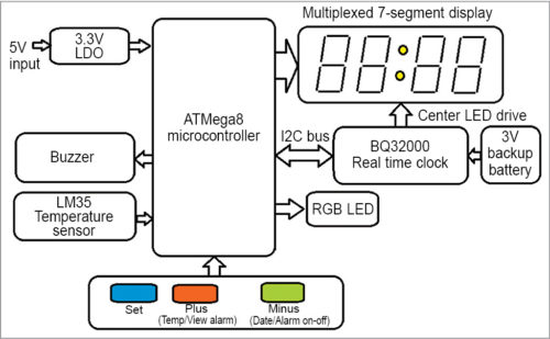
To sense the room temperature, a temperature sensor is used. Its output is an analogue signal proportional to the temperature. This signal is fed to one of the analogue-to-digital converter channels of the microcontroller. The user inputs are sensed by three momentary push-to-on switches, which are used to set/check various parameters of the digital clock like alarm, date, etc.
Time keeping is done by a separate real-time clock (RTC) chip that is interfaced to the microcontroller via I2C bus. The RTC is also powered by a backup battery, which keeps the time running even if the AC mains power fails.
The display section comprises four 7-segment displays, which are multiplexed to efficiently use the limited pins available on the microcontroller. The two centre LEDs between the two pairs of 7-segment displays are driven by the RTC clock. An RGB LED is used to display AM/PM and date. Finally, a buzzer is used to acknowledge pressing of the user button and provide alarm indication.
Circuit description
The clock circuit consists of power unit, LED and USB charging unit, main controller clock unit and 7-segment display unit.
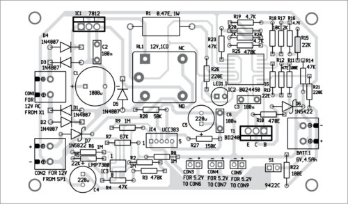
Power unit. Circuit diagram of the power unit is shown in Fig. 3. Here 230V AC mains is first converted into 12V AC using a step-down transformer. This 12V AC is converted into around 17V DC using diodes D1 though D4 in bridge configuration. This DC is further smoothened using a 1000µF electrolytic capacitor (C1) that acts as a first-order low-pass filter. Ceramic capacitor C2 is used for further stability of the 7812 regulator (IC1).
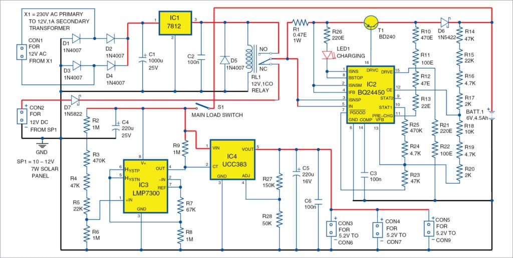
The linear regulator IC1 is used to derive regulated 12V DC, which is fed to the relay coil and also to the normally-open contacts of relay RL1. A 10-12V, 7-watt solar panel (SP1) is used to harness solar power. The electric power from the solar panel is fed to the normally-closed (NC) contacts of relay RL1 with a bypass diode (D7) in series.Diode D7 creates a voltage drop in the solar panel’s output, so it is recommended to use a diode that has the least forward dropout voltage, such as Schottky diode 1N5822. Diode D5, connected in parallel to the relay, prevents back emf of the relay coil from harming rest of the circuitry. Now, as the solar panel’s output is fed to NC contacts of the relay, when AC mains power is not available, the relay de-energises and thus solar power directly feeds the charging circuitry.
When AC mains power is available, the relay energises and thus the mains-derived 12V DC passes through the relay, cutting off the solar power. This way, during low solar power or night times, the user can charge the digital clock using AC mains power.
The common terminal of the relay is connected to the charging circuitry, which comprises BQ24450 (IC2). IC BQ24450 contains all the necessary circuitry to optimally control charging of valve-regulated lead-acid batteries. It controls the charging current as well as the charging voltage to safely and efficiently charge the battery, thus maximising battery capacity and life.
Here, IC BQ24450 is configured as a simple constant-voltage float charge controller for the 6V, 4.5Ah battery. It is so flexible that it can be programmed in various configurations to suit different charging currents and voltages for batteries of different capacities. Only an external pass transistor and very few external passive components are required along with the IC to implement a charger for sealed lead-acid batteries.
Here, a BD240 pnp transistor (T1) is used to drive the battery charging power. Before proceeding to battery charger programming, please refer to the datasheet of BQ24450. Note that charging rate can be 0.05C to 0.3C. We will use charging rate (Imax-chg) = 0.13C = 600mA (approx).
In programming, there are parameters to implement a dual-level charger for the given battery chemistry. The first step is to decide the value of current in the voltage divider resistor string in float mode. It should be substantially higher than the input bias current in CE and VFB pins and the leakage current in STAT1 pin of BQ24450, but low enough so that the voltage on PGOOD pin does not introduce errors. A value of 50µA is suitable. Readers interested in calculations may go through the calculations_charging.doc file included in the EFY DVD of this month.
LED1 in the BQ24450 circuitry displays the battery charging status. Schottky diode D6 prevents the back current leakage from the battery. Thereafter the circuit feeds the lead-acid battery. Next, the battery rail goes to the low-voltage detection circuit and IC UCC383 (IC4) in series with a mains mechanical load switch (S1).
The low-voltage-battery detection circuit is built around comparator LMP7300 (IC3), which has an internal reference of 2.048 volts. The voltage at which the battery should disconnect from the load is around 1.75V per cell, which means 5.25V for three-cell batteries.
The comparator has open-collector output, which goes low when the battery voltage drops below 5.25V. The comparator output goes to CT pin of IC4 in the next stage. Thus whenever the battery voltage goes below 5.25 volts, the comparator output goes low. This, in turn, switches IC4 off, shutting down all the loads connected to the battery and thus preventing the battery from discharging further.
The potential divider network comprising resistors R2 through R6 establishes 2.048V at the non-inverting terminal of comparator IC3 when the battery rail reaches 5.25V. It is compared with the voltage at the inverting terminal of the comparator, which is directly connected to the reference output of LMP7300. Further, a combined negative and positive hysteresis of about 300mV in total is programmed to LMP7300 through R7 and R8, so that the comparator output does not fluctuate when the battery voltage reaches the exact crossing point of the comparator’s reference potential.
The UCC383 LDO is capable of driving loads up to 3A with a maximum dropout of 0.45 volts, which is excellent for this application. VIN pin accepts the battery rail, which nominally varies in the range of 6 to 7.5 volts while charging and 5.25 to 6 volts during normal usage.
Through resistors R27 and R28, the output voltage of IC4 is set to 5V. Capacitors C4 through C6 are used for stability of IC4. The 5V rail thus obtained is used to power the rest of the circuit.
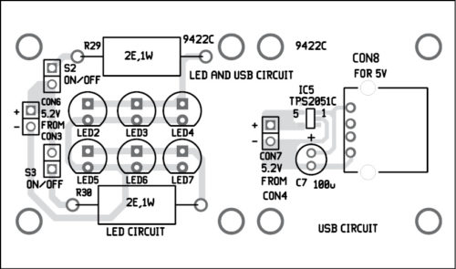
LEDs and USB charging. Circuit connections for power LEDs and the USB charging socket are shown in Fig. 4.
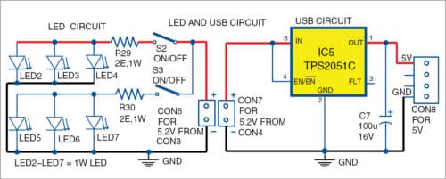
Here two pairs of 3×1-watt power LEDs are used for lighting application. A 2-ohm, 1W current-limiting resistor is used to limit current in each pair of LED channels in series with on/off switches S2 and S3. These LED channels receive power directly from the non-current-limited 5V rail (from the power unit). TPS2051C, which is a 500mA current-limited load switch, is used to drive a 500mA-limited 5V rail to power/charge the USB application.
The circuit is built around ATmega8 (IC8) microcontroller. IC8 is used to update the display, sense user inputs and take decisions. ATmega8 has 8kB of in-system programmable Flash with read-while-write capabilities, 512 bytes of EEPROM, 1kB of SRAM, 23 general-purpose input/output (I/O) lines, 32 general-purpose working registers, three flexible timers/counters with compare modes, internal and external interrupts, a serial programmable USART, a byte-oriented two-wire serial interface, a 6-channel analogue-to-digital converter (ADC) with 10-bit accuracy, a programmable watchdog timer with internal oscillator, an SPI serial port and five software-selectable power-saving modes, which are sufficient enough for this application.
A separate in-circuit serial programming port (CON12) is available for programming the microcontroller. Time keeping is done by RTC chip BQ32000 (IC7), which provides an automatic backup supply using a 3V battery. IC BQ32000 has a programmable calibration adjustment from –63ppm to +126ppm, so that it can also be used with low-quality crystals. It includes automatic leap-year compensation as well. The RTC chip is connected to the microcontroller via the I2C bus. This project uses a 3V CR2032 lithium cell for the backup supply.
For the internal oscillator functioning, a 32.768kHz crystal is used at OSC0 and OSC1 pins of IC7. IRQ pin on the RTC chip is connected to ATmega8 on port pin PD2 and is also responsible for seconds indication through the two LEDs (LED7 and LED8) that are located between the two 7-segment display pairs. Anodes of the two coloured LEDs (in parallel) are connected to IRQ pin, while the cathode is connected to ground on CON13. Three momentary push-to-on switches (S4 through S6) are connected to pins PD3, PC1 and PC2 of IC8, respectively.
Analogue temperature sensor LM35 (IC9) is used for room temperature sensing. The analogue signal output of IC LM35 is proportional to the temperature by the relationship 10mV/degree Celsius. It is interfaced to the ADC of the microcontroller. The sensor is connected to the ADC channel 3 (PC3) on ATmega8.
For display, four multiplexed common-cathode 7-segment displays (DIS1 through DIS4) are connected via CON10. Their individual cathode pins are connected to CON11, and driven by transistors T2 through T5. The RGB1 LED is connected to PB3, PB4 and PB5 pins of IC8. The active-low RESET pin on ATmega8 is pulled up by a 10-kilo-ohm resistor (R31) and also tied to a 10µF electrolytic capacitor (C12) to prevent the controller from regenerative resetting during supply transients. AVREF pin, reference in/out pin for the ADC, is tied to a 100nF ceramic capacitor (C13) for stability, while AVCC (pin 20) and AGND (pin 22) are power supply pins for the ADC circuitry on the microcontroller. VCC (7) and GND (8) are power pins for the rest of the circuitry on the microcontroller.
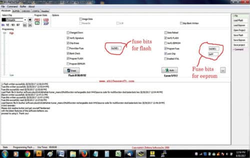
You need not connect any crystal to the microcontroller as its internal 1MHz R-C oscillator is used here. So it is important to set correct fuse bits on ATmega8 to configure it for the 1MHz internal R-C oscillator.
TPS73733 LDO IC (IC6) is used to power the clock circuit. It gets input from non-current-limited 5.2V rail of the power section. TPS73733 is a 3.3V, 1A regulator with a maximum input voltage of 5.5 volts. EN pin is used to enable the LDO, however here we have tied it directly to IN pin for continuous operation. Capacitors C8 through C11 are used for stability of the LDO. An external capacitor (C9) connected to NR/FB pin on the LDO bypasses noise generated by the internal bandgap, reducing LDO output noise to very low levels.
7-segment display unit. Circuit of the multiplexed 7-segment display unit is shown in Fig. 6.
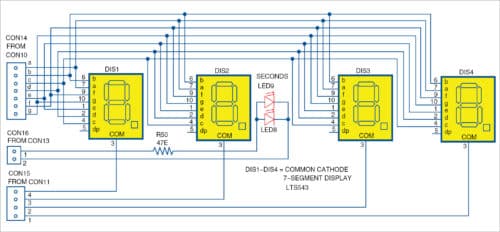
It comprises four 7-segment displays arranged in pairs of two: one pair (DIS1 and DIS2) on the left side to display variables like hours and date, and the other pair (DIS3 and DIS4) on the right side to display variables like minutes and month. CON14 through CON16 in the display unit are connected to display driving ports CON10, CON11 and CON13, respectively, in the main clock section (Fig. 5).
Software
The code for the ATmega8 microcontroller is written in BASIC language using BASCOM-AVR compiler. After initiating the code, allocate default values to the EEPROM from location one to four. The EEPROM is basically used to hold the user-settable alarm values. Starting from the first location, it holds alarm hours, then alarm minutes, then alarm PM and finally the alarm flag (which indicates whether alarm is on or not).You need to declare subroutines to clear 7-segment displays, read RTC chip, display value setting, etc. After this, configure the ADC to run in single-mode with auto prescaler and internal 2.56V reference. Configure the directions of input-output ports and initialise them. Then configure I2C pins and initialise them.
Next, initialise timer0 for multiplexing the 7-segment display, timer1 for handling the alarm duration and timer2 for blinking the segments while the clock is in ‘Settings’ mode. After this, declare and initialise certain variables for ADC calculations, time seeking, etc. Then initialise I2C pins, read EEPROM contents for alarm values and initiate an infinite super-loop where the RTC chip registers are read and displays are updated continuously. Also in the same loop, the user inputs are acknowledged and associated events like setting alarm on/off and displaying date-time are initiated. Also, the current time is compared against the alarm variables and alarm is initiated when the time is matched.
Download source folder
Note that while burning the hex file solarclock.hex to the microcontroller, the EEPROM file solarclock.eep must also be programmed. At EFY Lab, PROGISP programmer was used to program solarclock.hex and solarclock.eep. Fuse bits should be D9=high and E1=low as shown in Fig. 7.
The Digital clock
Charging
As mentioned earlier, the digital clock can be charged from solar power as well as AC mains power. Install a 10-12V, 7W solar panel on the rooftop such that it receives sufficient sunlight throughout the day. Route connections from the solar panel (SP1) carefully to the clock’s charging terminals, keeping in mind the correct polarity.
Solar power is more than enough to provide continuous power to the digital clock forever, and the digital clock can work for more than 60 hours on a single charge. But when solar power is not available on cloudy days or at night, users can charge the digital clock using 230V AC mains power. The solar panel rail is automatically cut off while charging through AC mains power. This way the digital clock never runs out of power. Switch S1 can be used to cut off all the load from the battery.
The two 3×1-watt LED modules can be individually switched on as required. Using the USB jack, you can charge all possible USB applications. Thus the project also functions as a solar-powered USB charger. The charging status is indicated by LED1 in the power unit, where a glowing LED means the battery is charging. The power unit circuit can automatically shut off the load when the battery voltage reaches the state of discharge.
Settings
The digital clock automatically turns on when the mains load switch (S1) is closed. The user-interface of the digital clock is designed such that only three buttons (S4 through S6) are required to set the various parameters like current time, hours and date-time, and to display the current date-time, set alarm and room temperature.
The Plus button can be used to increment the values in ‘Settings’ mode. Pressing it once during normal time display mode, first displays the room temperature and then the set alarm values. Thereafter, it reverts to normal time display with an acknowledgement beep.
Similarly, the Minus button can be used to decrement the values in ‘Settings’ mode. Pressing it once during normal time display mode first displays the current date on the left and the current month on the right, and then the current year. Thereafter, it reverts to normal time display with an acknowledgement beep.
To switch on/off the alarm, simply press and hold the Minus button for more than one second. If the display indicates AL-0, the alarm is turned off. AL-1 indicates the alarm is turned on.
To set the various parameters of the digital clock, press SET button once to bring it to ‘Settings’ menu. In ‘Settings’ menu, use Plus and Minus keys to increment and decrement the current values, respectively. The corresponding pair of 7-segment displays starts blinking. Pressing Set button again brings the digital clock into the next parameter setting mode and so on until the normal time is displayed. On pressing Set button once, the following seven settings are displayed:
1. Set current hours
2. Set current minutes: After setting the current hours and minutes, SET is displayed on the display
3. Set month
4. Set date
5. Set year. After setting month, date and year SET is displayed on the display
6. Set alarm hours
7. Set alarm minutes. After setting alarm hours and minutes SET is displayed on the display
To switch off the running alarm, press any of the three buttons once. Green colour on the RGB1 LED indicates AM, blue indicates PM and red indicates that date is displayed.
Construction and testing
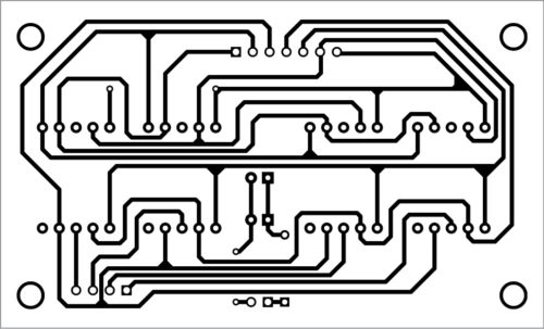
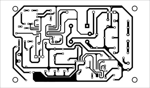
An actual-size PCB layout of the power unit (in Fig. 3) is shown in Fig. 8 and its components layout in Fig. 9. After assembling the circuit on the PCB, connect CON1 to the secondary of transformer X1, and CON2 to 10-12V, 7W solar panel. Extend CON3 through CON5 to other sections using proper connectors. Enclose the PCB in a suitable cabinet.
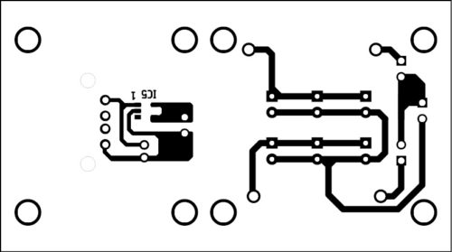
An actual-size PCB layout of the power LED and USB charging circuit (in Fig. 4) is shown in Fig. 10 and its components layout in Fig. 11. After assembling the circuit on the PCB, connect CON6 to CON3 in Fig. 3, and CON7 to CON4 in Fig. 3. Use CON8 for mobile charging through the USB cable. Affix all the LEDs (LED2 through LED7) on the top or front side of the cabinet.
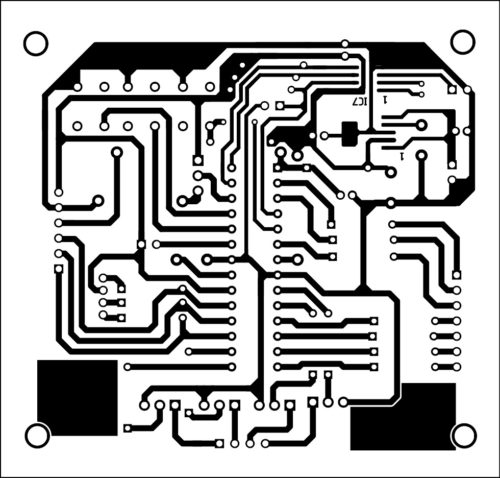
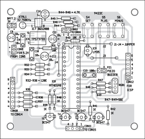
An actual-size PCB layout for the main clock controller circuit (in Fig. 5) is shown in Fig. 12 and its components layout in Fig. 13. After assembling the circuit on the PCB, connect CON9 to 5.2V from CON5 in Fig. 3. Connect the RGB1 LED and switches S1 through S6 on the front side of the cabinet.
An actual-size PCB layout of the 7-segment display unit (Fig. 6) is shown in Fig. 14 and its components layout in Fig. 15. After assembling the circuit on the PCB, connect CON14 to CON10, CON16 to CON13, and CON15 to CON11 from Fig. 5. Affix LED8 and LED9 on the PCB for seconds indication.