


 Often we require a squarewave signal generator with adjustable frequency, almost equal high and low output pulses and adjustable amplitudes. Here we present a simple, useful and low-cost signal generator built around NE555 timers. Using external switches, you can control or select frequency ranges as per your requirements. However, use of frequencies below 30kHz is recommended.
Circuit and working
This project is divided into two parts: Power supply and signal generator.
Power supply
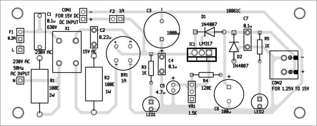
The circuit of the adjustable power supply for the signal generator is shown in Fig. 1. It is built around a step-down transformer (X1), a bridge rectifier (BR1), LM317 adjustable voltage regulator (IC1), two 1N4007 diodes (D1 and D2), two LEDs (LED1 and LED2) and a few other components.
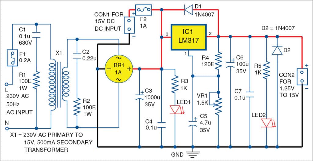
The power supply output available at connector CON2 is variable. You can vary the output from 1.25V to 15V using potmeter VR1. The variable power supply can be used for additional adjustment of the timers’ amplitude.
Signal generator
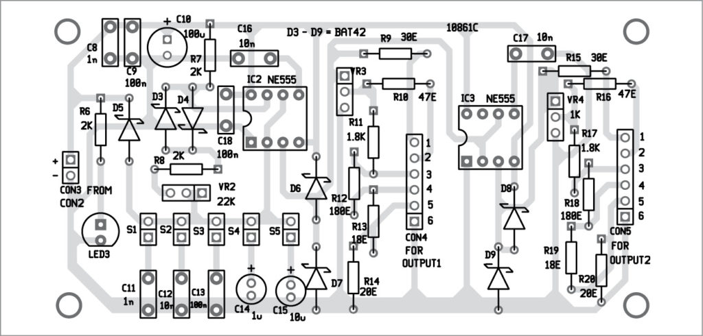
The circuit diagram of the signal generator is shown in Fig. 2. It is built around two NE555 timers (IC2 and IC3), an LED (LED3), seven BAT42 Schottky diodes (D3 through D9) and a few other components.
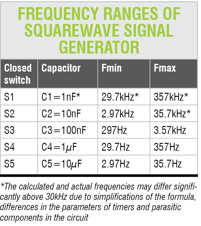

The signal generator produces forward and inverted signals through IC2 and IC3, respectively. Table below shows calculated frequency ranges of squarewave signals.
IC2 operates as a frequency generator. The frequency (F) is determined by components connected to pins 2, 6 and 7 of IC2 as follows:
F=1/{0.7(R7+R8+2xVR2)Cx}
where Cx may be 1nF, 10nF, 100nF, 1µF or 10µF.
Assuming switch S1 is closed and Cx=1nF and VR2=22-kilo-ohm, the minimal frequency (Fmin) is given as below:
Fmin=1/{0.7(2k+2k+2x22k)1nF}
=1/(0.7x48kx1nF)
=29762Hz
=29.7kHz approx.
When Cx=1nF and VR2=0-ohm, the maximal frequency (Fmax) is:
Fmax=1/(0.7x4kx1nF)
=1/(2800x1nF)
=1000000/2.8
=357142Hz
=357kHz approx.
Here, forward resistances and voltage drops of diodes D3 and D4 are neglected and inverse resistances of diodes assumed to be infinity.
The frequency signal output produced by IC2 is available at connector CON4. The amplitude of signals can be adjusted using potmeter VR3. Resistive dividers comprising R11 through R14 provide three more amplitudes. That is, the output frequency of IC2 is divided by 10, 100 and 1000. These frequencies are also available across CON4 at pins 3, 4 and 5, respectively.
IC3 works as an inverter. The amplitude of IC3’s inverted output available at CON5 can be adjusted using potmeter VR4. Resistive dividers comprising R17 through R20 provide three more amplitudes by dividing the inverted output by 10, 100 and 1000. These inverted outputs are available across CON5. Diodes D6 through D9 protect timer outputs from over-voltage and under-voltage.
Construction and testing
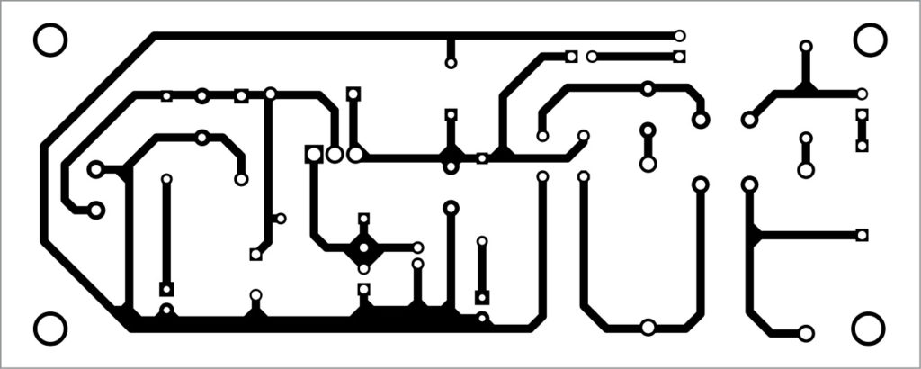
An actual-size PCB layout for the power supply is shown in Fig. 3 and its components layout in Fig. 4. After assembling the circuit on the PCB, connect the line (L) and neutral (N) to 230V AC mains supply. Variable power supply for the signal generator section is available at CON2. Connect LED1 and LED2 on the front panel for power-status indications. The circuit can be powered by either 230V AC, 50Hz mains power supply with transformer X1 or 15V DC power supply connected to CON1.
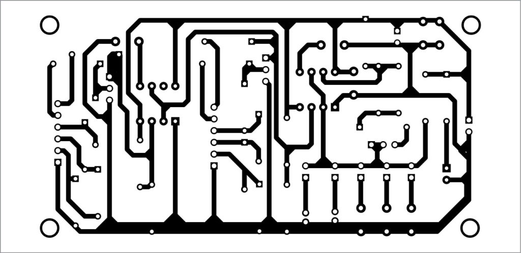
An actual-size PCB layout of the signal generator circuit (Fig. 2) is shown in Fig. 5 and its components layout in Fig. 6. After assembling the circuit on the PCB, connect variable power supply using a two-wire cable from CON2 to CON3. Connect LED3, switches S1 through S5 and potmeters VR2 through VR4 on the front panel for power-status indication, frequency selection and signal amplitude control, respectively.
Download PCB and component layout PDFs: click here
Note. For testing, you can also use 6V, 9V or 12V DC supply at CON3.
thanks very much
You are most welcome.
What is the working of inverter( Second 555 timer) part of the circuit ? Where does the square wave inverts in the circuit? Explain the working behind it.
Can you explain what we get on PIN 1 on CON4?