


Embedded Development Kit (EDK)
Embedded Development Kit (EDK) is a suite of tools and intellectual property (IP) that allows you to design and implement a complete embedded processor system in a Xilinx FPGA device. The aim of the EDK is to simplify the embedded-processor design process as it provides an umbrella covering all things related to embedded processor and its design. It may be mentioned here that EDK is specific to the FPGAs from Xilinx.
The EDK comprises two main components, namely, the Xilinx Platform Studio (XPS) and the Software Development Kit (SDK). XPS is used primarily for embedded-processor hardware system development, including configuration of the microprocessor, peripherals and the interconnection of these components, along with their respective property assignments. XPS has a base system builder (BSB) wizard that quickly and efficiently establishes a working design. The wizard is generally used to create the foundation of a new embedded design project.

SDK is the recommended software development environment for writing the software code for the embedded processors. Fig. 1 shows the embedded-processor design process.
Creating an EDK project
This section discusses how to create an EDK-driven design task to blink eight LEDs on and off at a frequency of 50Hz.
The different steps for designing the blinking of the LEDs are:
1. Open XPS by selecting Start → Programs → Xilinx ISE Design Suite 13.4_1 → EDK → Xilinx Platform Studio
2. From the dialogue box, select Create New Project Using Base System Builder
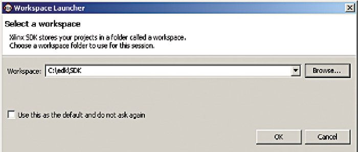
3. A window will appear titled Create New XPS Project Using BSB Wizard asking you to specify the folder to place the project. Set the desired path. (We have selected C:\edk as shown in Fig. 2.)
4. Then select the interconnect type, either as processor local bus (PLB) or advanced extensible interface (AXI), depending on the FPGA series you are using. As mentioned in the wizard, PLB is a legacy bus standard used by Xilinx that supports current FPGA families, including Spartan 6 and Virtex 6. It will not support new FPGA families. AXI is an interface standard recently adopted by Xilinx as the standard interface used for all current and future versions of Xilinx IP and tool flows. Choose among the two depending upon the FPGA family you are using. We are doing the design using Virtex-5, so we have selected PLB system. Click OK button
5. In the next window select ‘I would like to create a new design’ option and click Next, as shown in Fig. 3
6. A window appears asking the designer to select the board. If you have a standard development board from Xilinx mentioned in the list, select the first option ‘I would like to create a system for the following development board’ and fill in the vendor name as Xilinx and your board name. Otherwise, select the second option ‘I would like to create a system for a custom board’ and fill the board information. The design is being implemented on the ML501 board from Xilinx. As it is not mentioned in the Board Name in the first option, the second option has been selected and the relevant details are filled as shown in Fig. 4. Click Next
7. The next page, that is, the System Configuration page, asks you whether you want to build a single-processor system or a dual-processor system. Select Single-Processor System and click Next (Fig. 5)
8. The Processor Configuration page appears. Select 50.00MHz as the reference clock frequency. The Virstex-5 FPGAs do not have any hard processor, so Base System Builder will set up a MicroBlaze soft processor. Set the system clock frequency as 125.00MHz and local memory as 8kB, and click Next, as shown in Fig. 6
9. The Peripheral Configuration page appears through which we select the peripherals to put in the design. The peripherals will be connected to the MicroBlaze processor via the PLB, and they allow you to control and access features of the FPGA and external hardware. Click the Add Device button, select the IO Interface Type as GPIO and the device as LEDs, as shown in Fig. 7. Click OK
10. Select the GPIO Data Width as 8, as shown in Fig. 8, and click Next
11. Click Next on the Cache Configuration window
12. The Summary page (refer Fig. 9) gives you a summary of the design created by Base System Builder, showing the PLB memory map, peripherals and the files that will be generated
13. Since we are designing using a custom board, the window shown in Fig. 10 appears, indicating that the user needs to update the user constraints file and set the correct position of the FPGA in the JTAG chain. Click OK
14. The System Assembly View window appears, as shown in Fig. 11. The different regions in the window are explained below for understanding
15. The area marked as (A) contains the project information and has two tabs, namely, Project and IP Catalogue. The Project tab lists the project files like the Microprocessor Hardware Specification (MHS) file, User Constraints File (UCF), Bitgen Options File, iMPACT command file, implementation options file and the ELF file, and the project settings, including the device number, simulation model and netlist type
The MHS file defines the hardware components, that is, the configuration of the embedded-processor system, and includes the bus architecture, peripherals, processor, system connectivity and address space. It serves as an input to the platform generator (platgen) tool. The UCF specifies the timing and placement constraints for the FPGA design. The Bitgen Options File contains options for the bitstream generation tool. iMPACT command file is a script file used for downloading bit streams using iMPACT. The IP catalogue contains a list of the peripherals or IP cores that the project has access to. This tab is used when you want to instantiate IP cores into the design.