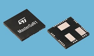
The solution ensures high power density and high-voltage that enables chargers and adapters to greatly reduce size and weight
 It is known that GaN technology enables devices such as smartphones, ultra-fast chargers and wireless chargers, USB-PD compact adapters for PCs and gaming, as well as in industrial applications like solar-energy storage systems, uninterruptible power supplies, or high-end OLED TVs and server cloud to handle more power as they become smaller, more lightweight, and more energy-efficient.
However, today’s GaN market is typically served by discrete power transistors and driver ICs that require designers to learn how to make them work together for better performance. While there is no harm in doing so, it results in slower time to market.
So here’s presenting the MasterGaN by STMicroelectronics that claims to be the world’s first platform that embeds a half-bridge driver-based on silicon technology along with a pair of gallium-nitride (GaN) transistors. The combination is expected to accelerate the development of next-generation compact and efficient chargers and power adapters for consumer and industrial applications up to 400W.
Enhanced Performance
The MasterGaN platform leverages STDRIVE 600V gate drivers and GaN High-Electron-Mobility Transistors (HEMT). It ensures high power density and high-voltage with over 2mm creepage distance between high-voltage and low-voltage pads.
The family of devices will span different GaN-transistor sizes (RDS(ON)) and will be offered as pin-compatible half-bridge products that let engineers scale successful designs with minimal hardware changes. By leveraging the low turn-on losses and absence of body-diode recovery that characterize GaN transistors, the products offer superior efficiency and overall performance enhancement in high-end, high-efficiency topologies such as flyback or forward with active clamp, resonant, bridgeless totem-pole PFC (power factor corrector) and other soft and hard-switching topologies used in AC-DC and DC-DC converters and DC-AC inverters.
Key Technicalities
The MasterGaN1 contains two normally-off transistors that feature closely matched timing parameters, 10A maximum current rating, and 150mΩ on-resistance (RDS(ON)). The logic inputs are compatible with signals from 3.3V to 15V. Comprehensive protection features are also built-in, including low-side and high-side UVLO protection, interlocking, a dedicated shutdown pin and over-temperature protection.
All these features help MasterGaN bypass various challenges, resulting in faster time to market and assured performance, together with a smaller footprint, simplified assembly, and increased reliability with fewer components. With GaN technology, chargers and adapters can cut 80 per cent of the size and 70 per cent of the weight of ordinary silicon-based solutions.
STMicroelectronics is launching the new platform with MasterGaN1, which contains two GaN power transistors connected as a half-bridge with integrated high-side and low-side drivers.
MasterGaN1 is in production now, in a 9mm x 9mm GQFN package and only 1mm high. It is available from ST distributors.
An evaluation board is also available to help jump-start customers’ power projects.


