


A new 2D heterostructure-based FET and memory device offers a more efficient and versatile alternative to conventional electronics.
Transistors, the linchpin of modern electronics like computers and smartphones, utilize semiconducting materials to control electrical flow by switching, detecting, and amplifying current. As traditional transistors approach their performance limits, engineers explore innovative designs using novel materials and configurations to enhance performance, shrink size, or introduce unique capabilities. Notably, reconfigurable field-effect transistors (FETs) are on the horizon, promising to streamline electronics by merging distinct functionalities, such as the traits of unipolar n- and p-type semiconductors, into one device.

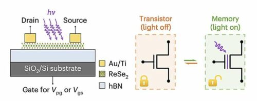
Researchers from National Tsing Hua University, National Chung Hsing University, and other Chinese institutes have developed a new reconfigurable device using a 2D heterostructure, which can function as a transistor and memory.
The reconfigurable transistor developed by the researchers can be adjusted through a light-activated process called photoinduced trapping. This technique allowed the team to dynamically manage the holes/electrons trapped between hBN and SiO2 within the device, thus altering the device’s channel doping setup. The team noted in their research that they’ve developed a reconfigurable FET using a hexagonal boron nitride/rhenium diselenide/hexagonal boron nitride (hBN/ReSe2/hBN) heterostructure, which boasts a non-volatile and adjustable polarity.
The team’s innovative design produces a transistor capable of operating across various charge transport regimes, potentially enhancing the efficiency of computing and memory devices across numerous electronics applications. The team mentioned in their research that a photoinduced trapping mechanism propels photoexcited holes or electrons into the interface between the hBN and the silicon dioxide substrate. The adaptable FET can transition between transistor and memory modes. Multiple FETs can design inverter, AND, OR, NAND, NOR, XOR, and XNOR circuits. Additionally, these devices can emulate synaptic functions suitable for neuromorphic computing systems in memory-mode operation.
In the future, the team’s adaptable transistor might be instrumental in creating high-performance circuits for neuromorphic computing. These systems are engineered to mimic the structure and operations of neural circuits found in the brain.
Reference: Meng-Yu Tsai et al, A reconfigurable transistor and memory based on a two-dimensional heterostructure and photoinduced trapping, Nature Electronics (2023). DOI: 10.1038/s41928-023-01034-7
