




Why are glass substrates gaining attention for AI chips? A method coats millions of tiny holes needed to connect advanced chip packages.
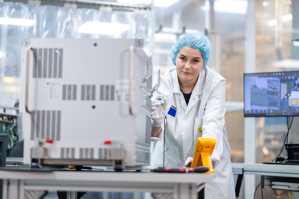
TRUMPF has developed an industrial high-power impulse magnetron sputtering (HiPIMS) process to coat the microscopic through-holes in glass substrates being considered for next-generation AI chip packaging.
As AI processors become more powerful, advanced packaging is becoming increasingly important for fitting more computing capability into smaller spaces. Glass substrates can support higher integration and faster signal transmission, but using them requires manufacturers to create and electrically connect millions of microscopic holes through the material.
These through-glass vias (TGVs) are particularly challenging to coat because the structures are extremely narrow and deep. Incomplete or uneven conductive coatings can make an entire glass panel unusable, making process consistency and manufacturing yield critical for high-volume production.
The HiPIMS approach addresses this by generating a highly ionised plasma containing a higher proportion of electrically charged particles than conventional coating methods. Electric and magnetic fields can then control these ions and direct them into deep, narrow structures.
This enables conductive material to be deposited more uniformly along the structures, including within deep trenches. The higher ionisation also increases the density of deposited material, improving coating quality and process stability.
The technology is intended to make glass-substrate packaging more suitable for series production by improving the consistency of TGV coating and reducing defects that can affect manufacturing yield.
The packaging process can involve several additional technologies. TRUMPF also develops ultrashort-pulse lasers for creating through-glass vias and plasma power supplies used in semiconductor coating and etching processes.
Together, these processes address different stages of glass-substrate manufacturing, from creating microscopic vias in the substrate to depositing conductive material within them.
Glass substrates are being explored for advanced packaging because they can enable higher-density interconnects and improved signal transmission for demanding applications such as AI processors, data-centre hardware, and high-performance computing.
The development highlights a key manufacturing challenge behind next-generation AI hardware in advanced packaging materials which require equally advanced processes to turn their theoretical benefits into reliable, high-yield production.

