


A new fabrication approach enables ultra-narrow 2D transistors to retain high performance at smaller dimensions.
Researchers at Stanford University have developed a novel method of manufacture where ultra-narrow nanoribbon transistors retain high performance levels in spite of decreasing the widths. The study was published in Nature Nanotechnology and describes a new design and multi-step etching process which highlights the potential of monolayer two-dimensional semiconductors in manufacturing of future ultra-small electronics.

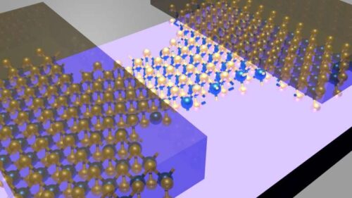
“We wanted to reduce 2D transistors in all dimensions, including width,” Eric Pop, senior author of the paper, told Tech Xplore. “Using a monolayer 2D semiconductor, the channel is automatically sub-nanometer thin, but to be technologically relevant, such transistors should also be very small in both length and width.”
“Another important part of our approach to reach the narrowest widths was how we etched the transistor channels,” said Anton Persson, co-first author of the paper. “Instead of etching the channel in one step, we used two separate etching steps, which etched the channel from opposite sides. This allowed us to form narrower channels than with the conventional one-step approach.”
Transistors have been created using three different monolayer two-dimensional semiconductors: MoS₂, WS₂ and WSe₂. According to the electrical measurements, all transistors demonstrated good transistor properties at narrow channels, with on-state currents of 560 µA/µm for n-type MoS₂, 420 µA/µm for n-type WS₂ and 130 µA/µm for p-type WSe₂. In addition, the researchers proved that decreasing the channel width did not affect the off-state leakage of the devices.

“We found that nothing dramatic happens when the transistors become very narrow,” said Persson. “We were concerned that the etched-out edges of these semiconductors would cause problems, but the devices still behaved well or at least similarly to their wider counterparts. This suggests that these monolayer 2D semiconductor channels are relatively robust when scaled down in width.”
To prevent nanoribbon delamination during fabrication, researchers have patterned the monolayers into a dog-bone like shape and integrated metal contacts at wider regions to work as anchors. Moreover, researchers used a two-step etching process, etching the channels from opposite sides enabled narrower channels than the traditional single-step approach.
“Understanding how various strains and defects impact these ultra-scaled 2D nanoribbons will also be critical, which will require sophisticated materials characterization approaches,” added Tara Peña, co-first author of the paper.
