


Scientists have developed a new method to create high-quality piezoelectric thin films, by showing electrons to remove impurities from these films.
Researchers at Empa, Switzerland have developed high-quality piezoelectric thin films, vital components in smartphones, RF filters, sensors, and emerging quantum devices. The new process, named Synchronized Floating Potential HiPIMS (SFP-HiPIMS), overcomes a major limitation that previously prevented very clean piezoelectric thin film deposition on non-conductive substrates at low temperatures.

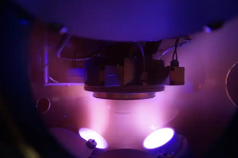
This innovation enables precise control of ion acceleration during High Power Impulse Magnetron Sputtering (HiPIMS), a method known for producing dense, durable coatings. Earlier, attempts to use HiPIMS for piezoelectric films failed due to contamination by argon gas, which compromised performance and electrical reliability.
Empa’s solution lies in perfect timing. By applying voltage to the substrate at just the right moment, only the desired metal ions are accelerated, while argon ions are left out. For insulating substrates like glass or sapphire, where voltage application isn’t feasible, the team used the magnetron’s own pulse to trigger an “electron shower,” which temporarily charges the surface, enabling selective ion attraction without contamination.
The ability to deposit high-performance films at low temperatures is particularly significant for the semiconductor industry, where many components cannot tolerate heat. It also allows thin-film integration on a wider range of materials, expanding possibilities for miniaturised electronics, optical devices, and next-gen quantum systems.
Empa has filed a patent for the process and published the findings in Nature Communications. Further work is underway to adapt the method for ferroelectric films and to scale up applications through partnerships with research institutes and industry.