


The technique avoids toxic byproducts from conventional halogen gases, cutting environmental impact while advancing semiconductor scaling.
Researchers from Japan and Taiwan have demonstrated a halogen-free plasma technique capable of etching hafnium oxide (HfO2) films with atomic-level precision, marking a significant step for next-generation semiconductor manufacturing. Reported in Small Science, the process achieves smooth, uniform surfaces at room temperature without relying on toxic halogen-based gases, which are widely used in conventional plasma etching.

HfO2 is already a cornerstone material in advanced electronics, valued for its high dielectric constant, thermal stability, and wide band gap. These properties make it an essential candidate for ultrathin gate insulators in 2D transistors and next-gen memory devices. Yet its strong hafnium–oxygen bonds also make HfO2 notoriously difficult to etch with both precision and surface smoothness.
Traditional plasma-enhanced atomic layer etching (ALE) methods address this using halogen gases—typically fluorine or chlorine—combined with energetic ion bombardment. While effective, the approach has drawbacks. Halogen gases are toxic and environmentally damaging, while their byproducts often have low volatility, clinging to reactor walls or device sidewalls and degrading performance.
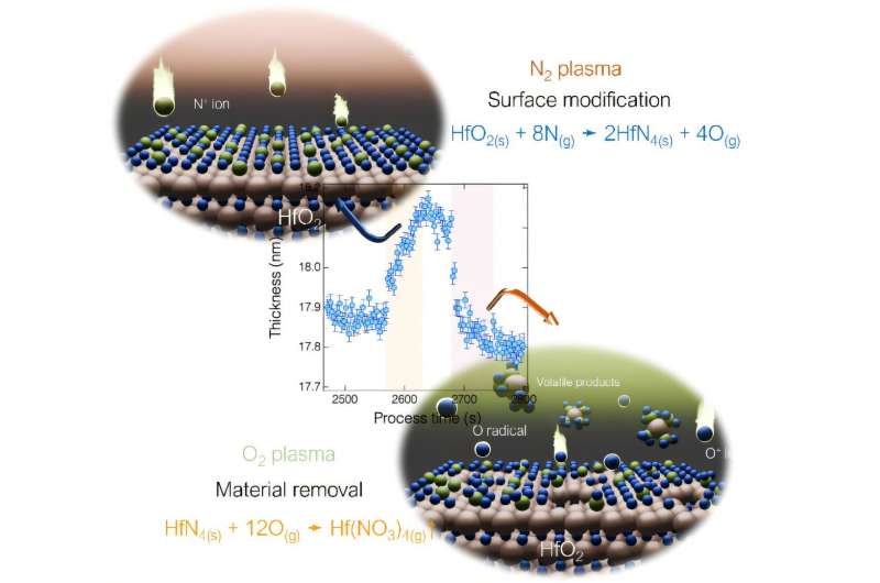
The team, led by Nagoya University’s Shih-Nan Hsiao and Masaru Hori in collaboration with Ming Chi University of Technology, designed a two-step cyclic method that replaces halogens with nitrogen and oxygen plasmas. In the first stage, N⁺ ions bombard the HfO2 surface, bonding nitrogen to the film. In the second, an O2 plasma strips away the nitrogen-bonded layer via a self-limiting reaction. Each cycle removes just 0.023 to 0.107 nanometers of material, enabling subatomic precision.
Surface analysis using infrared spectroscopy and X-ray photoelectron spectroscopy confirmed that nitrogen atoms temporarily replace oxygen atoms during the cycle before decomposing into volatile byproducts under oxygen plasma. Beyond etching, the method also improves surface morphology: after 20 cycles, roughness was reduced by 60%.
Crucially, the process operates at room temperature, saving energy and simplifying integration into semiconductor fabs. It also avoids halogen-based residues, supporting cleaner, more sustainable manufacturing.
As semiconductor dimensions shrink to just a few nanometers, techniques like this will be essential to maintain device performance while reducing environmental impact. The study establishes the first halogen-free atomic-level etching route for HfO2, potentially setting a model for processing other hard-to-etch materials in advanced microelectronics.
