- Researchers at POSTECH have successfully mass-produced world-first metalens for visible light.
- Mass production of metalens could accelerate commercialization in future.
Metalens, a nanostructured array, may eliminate camera bumps on smartphones. Despite being named a top 10 future technology by the World Economic Forum and receiving much attention in the scientific community, its precise production techniques and cost pose challenges for scalable manufacturing.
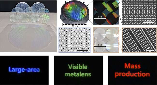
A team of researchers from POSTECH led by Professor Junsuk Rho (Department of Mechanical Engineering, Department of Chemical Engineering) have successfully mass-produced world-first metalens for visible light.

To overcome the limitations of the fabrication process, the team utilized a combination of two techniques commonly used in semiconductor and display manufacturing. The first technique, photolithography, uses light to pattern a substrate, similar to photography. The second technique, nanoimprint lithography, involves using a stamp with nano-sized patterns to print patterns onto a substrate. Initially, the researchers utilized electron beam lithography to generate a single pattern and then utilized deep-ultraviolet ArF photolithography to duplicate the pattern, resulting in a 12-inch master stamp. Subsequently, using the master stamp and nanoimprint lithography, they produced metalenses with a diameter of 1 cm at a high pace, overcoming the limitations of the fabrication process.
Metalenses produced using conventional nanoimprint technology had low refractive indices, which led to low-efficiency levels of around 10%. Achieving higher efficiency required significant costs. However, the research team improved the lens efficiency up to 90% by coating the lens with a very thin layer of titanium dioxide (TiO2) of about 20 nanometers. By combining the two technologies, the team could produce high-performance metalenses on a large scale with a simple process. In addition, the team showcased the practical applications of metalenses by developing lightweight virtual reality (VR) devices that display red, green, and blue images. With the successful mass production of high-performance metalenses, there is an expectation for accelerating their commercialization.
As per the researchers, the study shows how to commercialize meta-material research after 20 years and mass-produce advanced metalenses for visible light on a wafer scale.
Reference : Joohoon Kim et al, Scalable manufacturing of high-index atomic layer–polymer hybrid metasurfaces for metaphotonics in the visible, Nature Materials (2023). DOI: 10.1038/s41563-023-01485-5