


For semiconductor manufacturers, this explains how a single metrology platform measures wiring and packaging metals to improve yield and process control.
As semiconductor devices scale for AI computing, advanced packaging and high density interconnects, manufacturers face growing challenges in measuring ultra thin metal layers and micro scale bump structures. Conventional inspection methods often require multiple tools and struggle with non destructive analysis of complex metal stacks, impacting yield and process control.
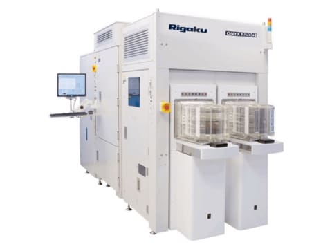
Addressing this need, Rigaku Corporation has introduced the ONYX 3200, a semiconductor metrology system designed to measure metal film thickness, composition and bump structures across wafer level back end and packaging processes on a single platform. The system supports inspection of metal layers thinner than a human hair and bumps smaller than 10 micrometers, which are increasingly common in modern chip wiring and interconnect architectures.
The system integrates optical and X-ray based measurement techniques to enable complete metal inspection without sample damage. This approach allows manufacturers to evaluate complex bump structures that previously required multiple inspection systems, improving consistency and throughput in production environments.
Key features include:
- Measures metal thickness, composition and bump structures on one platform
- Supports non destructive inspection for BEOL and advanced packaging processes
- 3D confocal scanner enables precise bump shape and height measurement
- Dual head microfocus X ray source detects silver content as low as 2 percent in SnAg bumps
- Enables calculation of lower metal layers by combining optical and X ray data
“Demand for accurate, non destructive metal inspection continues to rise as interconnect structures become more complex,” says Jun Kawakami, CEO of Rigaku Corporation, as a broader deployment and packaging complexity continues to increase.