


Researchers at the Centre for Nano and Soft Matter Sciences have designed a functional memory using tin oxide slanted nanorod arrays for high-density and high-efficiency computing systems.
New photonic memory based on tin oxide slanted nanorod arrays can modulate switching characteristics with optical and electrical stimuli. It has the potential for high-density and high-efficiency computing systems. A new class of data storage devices, including memristors, is being vigorously pursued to overcome the limitations of current memory technologies. Memristors use electrical signals to store and process data.

Researchers at the Centre for Nano and Soft Matter Sciences (CeNS), Bangalore, have designed a functional memory using tin oxide slanted nanorod arrays with high potential for high-density and high-efficiency computing systems. The resistive memory can modulate switching characteristics using optical and electrical stimuli, including multi level cell operation.
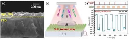
The team developed a photonic memory using tin oxide slanted nanorod arrays as an active layer. Tin oxide nanostructures were prepared using the glancing angle deposition (GLAD) technique with electron-beam evaporation. Electron-beam evaporation is a physical vapor deposition method where a focused electron beam vaporizes the target material and deposits it onto the substrate. GLAD manipulates substrate coordinates to prepare complex nanostructures. The memory devices showed good switching characteristics, including low operating voltages, moderate ON/OFF ratio, longer endurance, and better retention with a self-compliance effect in the dark. Interestingly, an unusual negative photo response with an enlarged ON/OFF ratio greater than 107 and faster response time is observed under various illuminations.
The devices exhibit electrical SET and optical RESET, where a voltage bias switches them to a low resistance state (LRS), and exposure to light switches them to a high resistance state (HRS). Multiple low and high resistance states are achieved by modulating the programming current and optical stimulus, with oxygen vacancies responsible for optically-stimulated resistance switching. Applying electrical bias forms nanoscale conductive filaments composed of oxygen vacancies, and photo-stimulated recombination ruptures the filaments. Thus, the local conductivity of the tin oxide nanorod array can be modified by the interplay between electrical and optical means.

The researchers believe that the study can facilitate the design of photonic memories using metal oxide nanostructures and explore their applications in optoelectronics and artificial visual memory.
Reference : Publication link: https://doi.org/10.1021/acsami.2c22362