
A tabletop chip-making system can print multiple nanoscale layers at once, cutting fabrication time from days to minutes and lowering research costs.
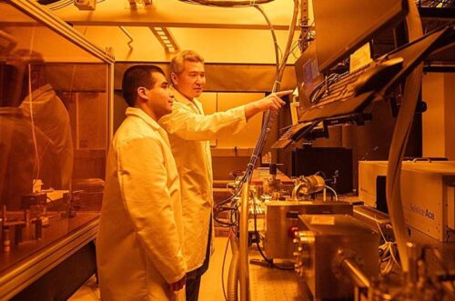
Researchers at the University of Texas at Austin have developed a tabletop extreme ultraviolet (EUV) lithography system that could make semiconductor research more accessible by reducing the cost and complexity of chip fabrication tools.

The compact system is paired with a volumetric 3D patterning technique that enables multiple nanoscale layers to be printed simultaneously. The approach addresses a limitation of conventional EUV lithography, which typically builds three-dimensional structures one layer at a time, a process that can take days to complete.
EUV lithography is a manufacturing technology used to create semiconductor circuits on silicon wafers. The process is used in the production of chips found in smartphones, computers, and other electronic devices. However, commercial EUV systems are among the most expensive tools in semiconductor manufacturing, often costing more than $200 million and occupying an entire room.
To lower that barrier, researchers from the Cockrell School of Engineering stripped the conventional EUV setup down to its essential components and built a smaller, modular version designed for laboratory use. The reduced footprint and lower cost could allow more research groups to experiment with semiconductor materials and manufacturing processes.
The new system works alongside a parallel printing method that exposes multiple layers of a nanostructure at the same time. Researchers say that while actual exposure in traditional lithography may be relatively quick, the repeated processing required between layers significantly increases manufacturing time. By eliminating much of that repetition, the new approach can reduce fabrication times from days to minutes.
The platform has already been tested with EUV-sensitive materials developed by researchers at the University of Texas at Dallas and Johns Hopkins University. The work is part of the National Science Foundation’s Future of Semiconductors (FuSe2) program, which aims to reduce the cost of semiconductor research and development.
At its current stage, the process can create periodic nanoscale structures, making it suitable for applications such as memory devices and photonic components. Researchers plan to expand the technology to support faster printing speeds and more complex semiconductor features in the future.
The ability to manufacture three-dimensional nanostructures could also have applications beyond electronics, including quantum computing, drug delivery systems, and the development of new materials.