


A new generation of programmable clocks promises to push system-level performance for next-gen networks and data-heavy platforms.
A fresh suite of programmable timing devices by Skyworks Solutions, Inc. has emerged that takes aim at one of the toughest challenges in modern digital systems: delivering ultra-low phase noise and jitter across diverse applications spanning high-speed networking, wireless radio access and data center interconnects. These clocks are the latest to combine advanced resonator technology with field-programmability to support demanding performance requirements from 5G/6G to multi-terabit optical links.

At the heart of the new solutions is integration of a bulk acoustic wave (BAW) frequency reference with a flexible multi-PLL and fractional divider timing architecture. By embedding the resonator on-chip, the devices eliminate the need for external quartz crystals, oscillators or VCXOs cutting board complexity and bill-of-materials costs while boosting reliability.
The main features are:
- Integrated BAW resonator removes the need for external crystal/XO/VCXO references.
- Ultra-low synchronous Ethernet jitter (~17 fs) for high-speed SerDes.
- Low phase noise (~–142 dBc/Hz) with IEEE 1588 Class C/D sync support.
- Common footprint and programmable interface for multiple clock roles.
- Factory and field programmability via integrated flash memory.
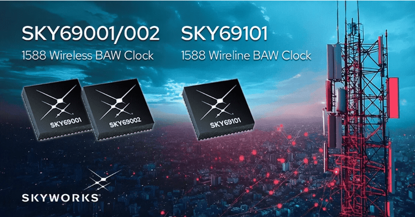
Two broad classes of clocks were introduced. The first targets jitter-attenuating roles in wireline and data center equipment where precision timing is essential. These deliver extremely low synchronous Ethernet jitter around 17 femtoseconds supporting high-speed PAM4 SerDes links used in 800 G, 1.2 T and 1.6 T optical networks and Data Center Interconnect applications.
The second class focuses on network synchronization for wireless systems. These clocks pair very low phase noise (≈ –142 dBc/Hz at 100 kHz offset) with IEEE 1588 Class C/D support, enabling precise timing distribution for modern radio access architectures such as massive MIMO and advanced 5G/6G base stations.
Both families share common hardware footprints and software interfaces, which simplifies development across timing roles. On-board flash memory enables factory and field programming of frequency plans, letting designers tailor clock behavior without hardware changes. Robust operation over a wide temperature range and efficient power consumption further extend applicability in challenging environments.
This move underscores broader trends in the industry toward tighter integration, greater flexibility and higher performance in timing components, factors that are increasingly critical as data throughput and synchronization demands continue to accelerate across telecom and compute infrastructure.
