


Researchers have developed a way to utilize two-dimensional materials on a silicon microchip to increase the device performance and yield.
Two-dimensional materials are substances with a thickness of a few nanometres or less. Electrons in these materials are free to move in the two-dimensional plane, but their restricted motion in the third direction is governed by quantum mechanics. Two-dimensional materials are expected to revolutionize the semiconductor industry. However, their technology readiness level is still very low because they mostly use synthesis and processing methods that are incompatible with industry, create the large devices on unfunctional substrates, and present poor variability and yield.

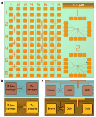
A team of researchers from King Abdullah University of Science and Technology (KAUST) led by Dr. Mario Lanza, associate professor of materials science and engineering, has successfully integrated two-dimensional materials on silicon microchips, and achieved excellent integration density, electronic performance and yield.
Researchers used a two-dimensional insulating material called multilayer hexagonal boron nitride (about 6 nanometers thick), and employed microchips containing silicon transistors of complementary metal-oxide-semiconductor (CMOS) technology—a type of technology that is present in every electronic product we use such as phones, computers, automobiles, medical machines and household appliances.
The resulting hybrid 2D/CMOS microchips exhibit high durability and special electronic properties that enable the fabrication of artificial neural networks with very low power consumption. They can successfully compute spiking neural networks (electrical stresses applied during very short time periods), a key component of current artificial intelligence systems that are increasing in demand. Most current devices are not suitable for implementing this type of neural network, and there is a market need to find new approaches.

The research could help companies reduce processing costs and energy. Most companies in the field of microchip manufacturing and artificial intelligence are aiming to create new hardware that reduces data processing time and energy consumption but have not yet found a suitable device.
Reference : Kaichen Zhu et al, Hybrid 2D/CMOS microchips for memristive applications, Nature (2023). DOI: 10.1038/s41586-023-05973-1