


Researchers at Pohang University of Science & Technology (POSTECH), South Korea, developed a high-performing p-type transistor using perovskite, a naturally occurring mineral of calcium titanate. This study was published in Nature Electronics in February 2022. The improved performance of these transistors has now enabled solution-processed perovskite transistors to be simply printed as semiconductor-like circuits.
Perovskite-based transistors combine the p-type semiconductors that exhibit hole mobilities with n-type semiconductors in order to control the current. However, fabricating p-type semiconductors has always been a challenge. Although the perovskite in the p-type semiconductor has excellent electrical conductivity, its reproducibility is poor and this has hindered its commercialization so far. Moreover, improving its electrical performance has also been an issue.

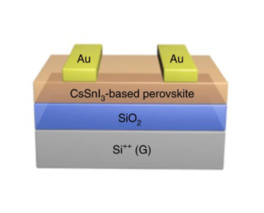
The research team led by Professor Yong-Young Noh and PhD candidates Ao Liu and Huihui Zhu (Department of Chemical Engineering), in collaboration with Professor Myung-Gil Kim (School of Advanced Materials Science and Engineering) of Sungkyunkwan University used the modified inorganic metal halide, Caesium Tin Triiodide (CsSnI3) to develop the p-type perovskite semiconductor. During their research, the resulting transistor recorded the highest performance among the perovskite semiconductor transistors that have been developed so far.
By making the material into a solution, the researchers succeeded in simply printing the p-type semiconductor transistor as if printing a document. This method is not only convenient but also cost-effective, which can lead to the commercialization of perovskite devices in the future.
“The newly developed semiconductor material and transistor can be widely applicable as logic circuits in high-end displays and in wearable electronic devices, and also be used in stacked electronic circuits and optoelectronic devices by stacking them vertically with silicon semiconductors,” explained Professor Yong-Young Noh on the significance of the study.
This approach could help lead to the development of high-performance p-channel transistors and complementary electronics that require only low-cost solution processes.
Read the entire study here.
