


By infusing semiconductors with gallium through atomic-scale precision, the team unlocked zero-resistance conductivity at cryogenic temperatures, opening doors to next-generation quantum chips and ultra-efficient electronics.
In an advancement for electronics and quantum technology, researchers from New York University have successfully turned the everyday semiconductor Germanium into a full-fledged superconductor — marking a milestone in material science that blends the best of both worlds.
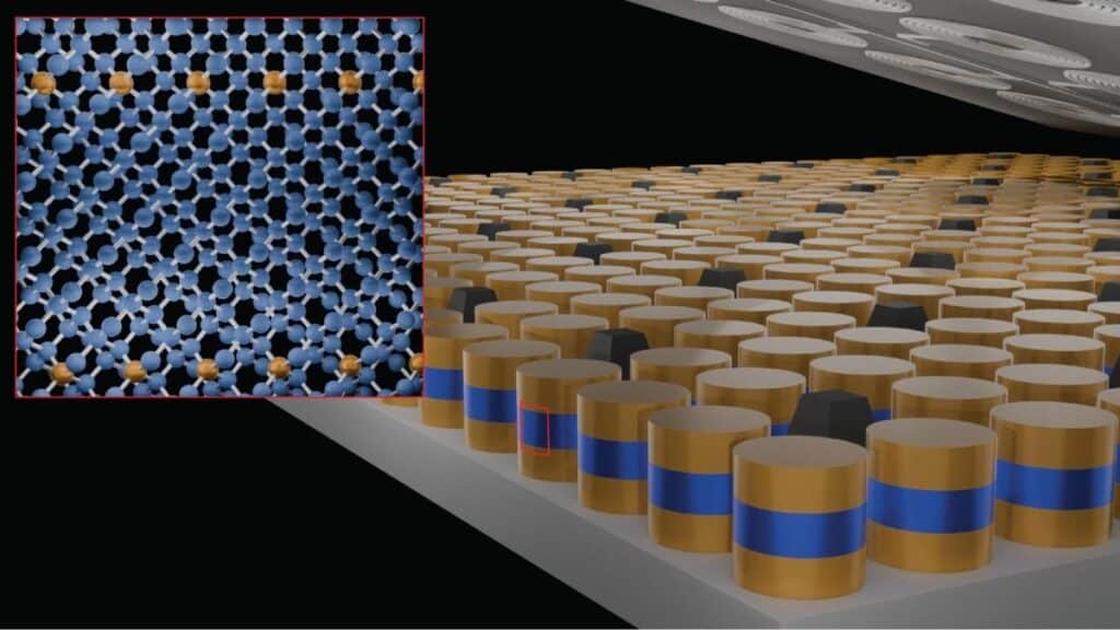
The team achieved superconductivity in germanium by using a molecular beam epitaxy process to infuse the element Gallium deep into the material’s crystal lattice. This ultra-precise method replaces germanium atoms with gallium at levels far higher than conventional doping allows — all while preserving the crystal’s structure. At around 3.5 Kelvin (about –453 °F), the material then conducts electricity with zero resistance.
Why is this a big deal? Germanium already serves as a staple semiconductor in chips, fiber optics and beyond. By making it superconducting, the material bridges a gap between technologies that rely on semiconductors (excellent for controlled switching) and superconductors (exceptional for loss-free current flow). The result opens avenues for ultra-efficient electronics, low-power cryogenic systems and quantum devices built at scale.
Until now, group IV semiconductors like silicon and germanium resisted superconductivity because it’s extremely demanding to orchestrate the crystal structure, electron count and purity needed. The researchers’ trick was to hyper-dope germanium with gallium, slightly deforming the lattice but keeping order enough for electron pairs to flow freely.
What comes next? Think quantum circuits where the semiconducting parts and superconducting parts are built in the same platform — removing barriers between two major technological domains. According to the team, this could enable sensors, quantum bits and low-power cryogenic electronics that are both scalable and compatible with existing semiconductor infrastructure.
Of course, challenges remain: operating at 3.5 K means cooling is still required, and integrating these novel films into real devices will test manufacturing robustness. But this breakthrough suggests the future of electronics may lie in hybrids — where the boundaries between semiconductors and superconductors fade.
