


Launched in 1996, the AVR core combines a rich instruction set with 32 general purpose working registers. All the 32 registers are directly connected to the Arithmetic Logic Unit (ALU), allowing two independent registers to be accessed in one single instruction executed in one clock cycle. The resulting architecture is more code efficient while achieving throughputs up to ten times faster than conventional CISC microcontrollers. AVR microcontrollers find many applications as embedded systems; they are also used in Arduino board designs. Here we go through ATmega16 pin diagram, block diagram, operating mode and features. But before talking about ATmega16 pin diagram, let’s first go through the Atmega16 block diagram.
ATmega16 Block Diagram
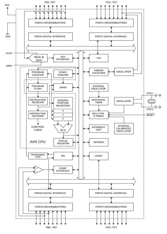
The ATmega16 is a low-power CMOS 8-bit microcontroller based on the AVR enhanced RISC architecture. By executing powerful instructions in a single clock cycle, the ATmega16 achieves throughputs approaching 1 MIPS per MHz allowing the system designer to optimize power consumption versus processing speed.

Features
- Advanced RISC Architecture
- 131 Powerful Instructions – Most Single-clock Cycle Execution
- 32 x 8 General Purpose Working Registers
- Fully Static Operation
- Up to 16 MIPS Throughput at 16 MHz
- On-chip 2-cycle Multiplier
- High Endurance Non-volatile Memory segments
- 16 Kbytes of In-System Self-Programmable Flash program memory
- 512 Bytes EEPROM
- 1 Kbyte Internal SRAM
- Write/Erase Cycles: 10,000 Flash/100,000 EEPROM
- Data retention: 20 years at 85°C/100 years at 25°C(1)
- Optional Boot Code Section with Independent Lock Bits
- In-System Programming by On-chip Boot Program
- True Read-While-Write Operation
- Programming Lock for Software Security
- JTAG (IEEE std. 1149.1 Compliant) Interface
- Boundary-scan Capabilities According to the JTAG Standard
- Extensive On-chip Debug Support
- Programming of Flash, EEPROM, Fuses, and Lock Bits through the JTAG Interface
- Peripheral Features
- Two 8-bit Timer/Counters with Separate Prescalers and Compare Modes
- One 16-bit Timer/Counter with Separate Prescaler, Compare Mode, and Capture Mode
- Real Time Counter with Separate Oscillator
- Four PWM Channels
- 8-channel, 10-bit ADC
- 8 Single-ended Channels
- 7 Differential Channels in TQFP Package Only
- 2 Differential Channels with Programmable Gain at 1x, 10x, or 200x
- Byte-oriented Two-wire Serial Interface
- Programmable Serial USART
- Master/Slave SPI Serial Interface
- Programmable Watchdog Timer with Separate On-chip Oscillator
- On-chip Analog Comparator
- Special Microcontroller Features
- Power-on Reset and Programmable Brown-out Detection
- Internal Calibrated RC Oscillator
- External and Internal Interrupt Sources
- Six Sleep Modes: Idle, ADC Noise Reduction, Power-save, Power-down, Standby and Extended Standby
- I/O and Packages
- 32 Programmable I/O Lines
- 40-pin PDIP, 44-lead TQFP, and 44-pad QFN/MLF
- Operating Voltages
- 7V – 5.5V for ATmega16L
- 5V – 5.5V for ATmega16
- Speed Grades
- 0 – 8 MHz for ATmega16L
- 0 – 16 MHz for ATmega16
- Power Consumption @ 1 MHz, 3V, and 25°C for ATmega16L
- Active: 1.1 mA
- Idle Mode: 0.35 mA
- Power-down Mode: < 1 µA
Let’s look at the ATmega16 pin diagram in detail.
ATmega16 Pin Diagram & Description
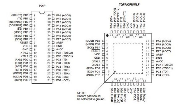
Detailed description of the ATmega16 pin diagram:
Vcc: Digital supply voltage
GND: Ground
Port A (PA7…PA0)
Port A serves as the analog inputs to the A/D Converter. Port A also serves as an 8-bit bi-directional I/O port, if the A/D Converter is not used. Port pins can provide internal pull-up resistors (selected for each bit). The Port A output buffers have symmetrical drive characteristics with both high sink and source capability. When pins PA0 to PA7 are used as inputs and are externally pulled low, they will source current if the internal pull-up resistors are activated. The Port A pins are tri-stated when a reset condition becomes active, even if the clock is not running.
Port B (PB7…PB0)
Port B is an 8-bit bi-directional I/O port with internal pull-up resistors (selected for each bit). The Port B output buffers have symmetrical drive characteristics with both high sink and source capability. As inputs, Port B pins that are externally pulled low will source current if the pull-up resistors are activated. The Port B pins are tri-stated when a reset condition becomes active, even if the clock is not running.
Port C (PC7…PC0)
Port C is an 8-bit bi-directional I/O port with internal pull-up resistors (selected for each bit). The Port C output buffers have symmetrical drive characteristics with both high sink and source capability. As inputs, Port C pins that are externally pulled low will source current if the pull-up resistors are activated. The Port C pins are tri-stated when a reset condition becomes active, even if the clock is not running. If the JTAG interface is enabled, the pull-up resistors on pins PC5(TDI), PC3(TMS) and PC2(TCK) will be activated even if a reset occurs.
Port D (PD7…PD0)
Port D is an 8-bit bi-directional I/O port with internal pull-up resistors (selected for each bit). The Port D output buffers have symmetrical drive characteristics with both high sink and source capability. As inputs, Port D pins that are externally pulled low will source current if the pull-up resistors are activated. The Port D pins are tri-stated when a reset condition becomes active, even if the clock is not running.
RESET
Reset Input. A low level on this pin for longer than the minimum pulse length will generate a reset, even if the clock is not running. The minimum pulse length is given in Table 15 on page 38. Shorter pulses are not guaranteed to generate a reset.
XTAL1: Input to the inverting Oscillator amplifier and input to the internal clock operating circuit.
XTAL2: Output from the inverting Oscillator amplifier.
AVcc: AVcc is the supply voltage pin for Port A and the A/D Converter. It should be externally connected to Vcc, even if the ADC is not used. If the ADC is used, it should be connected to VCC through a low-pass filter.
Aref: Aref is the analog reference pin for the A/D Converter.
Operating states
- The Idle mode stops the CPU while allowing the USART, two-wire interface, A/D Converter, SRAM, timer/counters, SPI port, and interrupt system to continue functioning.
- Power-down mode saves the register contents but freezes the Oscillator, disabling all other chip functions until the next External Interrupt or Hardware Reset.
- In Power-save mode, the Asynchronous Timer continues to run, allowing the user to maintain a timer base while the rest of the device is sleeping.
- ADC Noise Reduction mode stops the CPU and all I/O modules except Asynchronous Timer and ADC, to minimize switching noise during ADC conversions.
- In Standby mode, the crystal/resonator Oscillator is running while the rest of the device is sleeping. This allows very fast start-up combined with low-power consumption.
- In Extended Standby mode, both the main Oscillator and the Asynchronous Timer continue to run.
The on-chip ISP flash allows the program memory to be reprogrammed in-system through a SPI serial interface, by a conventional non-volatile memory programmer, or by an On-chip Boot program running on the AVR core. The boot program can use any interface to download the application program in the Application Flash memory. Software in the Boot Flash section will continue to run while the Application Flash section is updated, providing true Read-While-Write operation. By combining an 8-bit RISC CPU with In-System Self-Programmable Flash on a monolithic chip, the Atmel ATmega16 is a powerful microcontroller that provides a highly-flexible and cost-effective solution to many embedded control applications.
Full datasheet available here.
More basic article available in the learning corner.