


Chip design is a process of chip design and is an important part of electronics engineering.It involves several steps such as
- Architecture design
- Basic logic design
- Logic verification
- Physical Design Layout
- Physical Design Verification
- Fabrication and final testing
System on Chip (SoC) – A Latest Trend In Chip Design
Once we lived in the age of large scale and very large scale integrated circuits. Today they are becoming outmoded. Today we are living in the mania of nanotechnology. Semiconductor engineering deals with chip architectures, gates etc.

System on Chip (SoC) is a single chip for embedded systems. SoCs are used when performance , size, weight and power consumption is an issue. Traditionally the hardware part is made using the CAD tool and the software part is written with programming languages. (such as C++, Python etc.)
Today a complex SoC consists of billions of transistors fabricated together. Such SoCs mean seamless integration of numerous IPs performing different functions and operating at different frequencies. For next generation chips on chip isolation becomes extremely important. Higher chip integration results in more transistor switching and more noise. Grounding effects, shielding, on chip decoupling, and global wire delays are some of the factors to be considered for designing next generation chips.
Chip design is where the immutable meets intractable. From some viewpoints, every element in a chip design is open to modification, but in practice there are reactions to every action. The need to track those effects is why electronic design automation (EDA) was invented, and once you start to analyse a chip design at that level you soon appreciate the complexity machine learning approach.

With design sizes increasing, concurrently managing those parameters is more challenging. Chip designs should not have a negative impact on the power, performance and area (PPA) goals set by the customer.
During chip design every element in a chip needs modification due to technological advancements. But in practice such advancements may result in several disadvantages. This resulted in Electronic Chip Design automation ( EDA).
As technology is advancing, object oriented hardware design is becoming more effective. Every parameter in chip design is variable which results in wider design. Modern EDA tools are making chip design simpler. Integrated Chip (IC) designers should consider several.parameters such as thermal management requirements , signal integrity etc.
If such parameters are not considered it may result in severe problems and sometimes ends in IC design failure. Introduction of Machine Learning (ML) to EDA tools provided a great relief for designers. ML can check various parameters and even design a large portion of the system.
How ML Is Helping Chip Designers?
The EDA landscape shifts constantly in the semiconductor industry. ML brings a digital flow that makes correlation of all design data and makes EDA more efficient.
Machine Learning (ML) is a hot topic. Normally ML uses neural networks to analyse system data and identify solution pattern.Optimum among them is then selected to solve complex problems facing the industry. Today deep learning is helping chip manufacturing in all stages such as mask manufacturing, wafer design, FPGA design and PCB assembly automation. Alpha pruning techniques greatly help to minimise wastages during chip design.
Machine is tireless. It computes for a week and then comes up with an optimum neural network to design a chip. It is particularly helpful in SIMD.
Talking More About Chip Design
Newer chips are feature rich. For example 4550 has 13 channel 10 bit ADC . If design is simpler then reliability is more.
Network on Chip ( NoC) becomes absolutely necessary in solving complex situations. In designing such chips core – to – node mapping is absolutely necessary. This mapping as a result is a crucial design factor and should be considered in the early design stage.
Today microchips are made by building up layers of interconnected patterns on a silicon wafer. The microchip manufacturing process involves hundreds of steps and can take up to four months from design to mass production.
Now let us consider the defence electronics sector. Defence electronics are the hearts of several defence objects such as radar, missile launchers, drones, Laser range finders, Sonar domes, Torpedo launchers , Simulation softwares , submarines etc.
When designing high tech electronic systems for the military, standard electronic components simply won’t cut it. While many consumer goods are built on standard microchips, military systems operate on application specific integrated circuits (ASICS).
Commercial electronics are designed to last just a few years. For example Integrated chips found in Smart Tv is a commercial application specific chip that has a lifespan of 8 to 10 years. But military electronic systems need to last a few decades.Application specific chips fit inside military vehicles and other equipment that will be deployed to remote locations .Such chips need to last for 20 or even 30 years. These high tech chips must also be resilient enough to withstand high altitudes and extreme environments, such as deserts and the coldest regions. For military devices, reliability and dependability are more important.
Looking Closely At Biochips Design
The biochip is formed by dispensing optically transparent microdroplets of polyurethane-based hydrogel, having bio molecular probes covalently attached thereto, on to a substrate.
The biochips are mainly of three types: DNA microarray, protein microarray, and microfluidic chip.
Once the pharma world survived with inorganic chips.Trend is different today. Biochips are becoming popular day by day in molecular and pharma research laboratories.As such lab on a chip design is also becoming important for a chip designer.
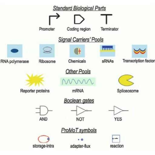
Designing of biochips is partly sometimes entirely different from designing an electronic chip such as a computer or a laptop chip. Here the circuit diagram does not work. Biochip designers must be conservant with various other symbols too.Some of the symbols used during biochip designing are given in the figure below.
While designing Biochips he has to consider several biological factors like biochem reaction mechanisms if he is designing biochips for drug invention. Suppose he is designing a biochip for internal human body application, then he has to consider various inside body parameters such as ph of gastric juice, ph of blood, blood pressure, inside body temperature etc.
Biochip devices today can automate laboratory procedures in biochemistry and molecular biology. Corresponding systems are revolutionising a diverse range of applications, e.g. air quality studies, point-of-care clinical diagnostics, drug discovery, and DNA sequencing-with an increasing market. For clinical diagnostics, it has been predicted that the world will soon see 15 billion diagnostic tests per year worldwide. Biochips are greatly used in clinical diagnostics.
Conclusion
The incorporation of machine learning helps manage the large amount of data the tiny chip produces. This branch of AI accelerates the processing and analysis of large datasets, finding patterns and associations, predicting precise outcomes, and aiding in rapid and efficient decision- making.
By including machine learning in chip design , the accuracy of analysis can be increased. Further it reduces the dependency on skilled analysts, which can also make the chip designing technology appealing .
By Vinayak Ramachandra Adkoli is a B. E. in Industrial Production and served as lecturer in three different polytechnics for 10 years. I am also a freelance writer and cartoonist.