


[stextbox id=”info” caption=”1. Photovoltaic cells” bgcolor=”61ABFF”]
In order to alleviate global warming by reducing greenhouse gas emission from combustion of fossil fuel, various countries are committed to curb 40-45 per cent carbon emission and increase the share of renewable energy to about 15 per cent of the total energy generated by 2020. This presents a big market opportunity for photovoltaic (PV) manufacturers.

More than 80 per cent of PV modules installed worldwide are made of crystalline silicon (c-Si). One of the main drawbacks of c-Si modules is their high cost due to use of expensive raw material, complicated manufacturing process and sophisticated equipment. Hence thin-film (TF) PV modules are rapidly gaining market shares because of their lower cost per watt, especially due to much lower use of the critical light-absorbing materials.
Thin-film PV cells are made from either amorphous silicon (a-Si) or copper indium gallium diselenide (CIGS) and organic photovoltaic. The research focuses on the key to fabricating low-cost thin-film solar cells, which includes controlling the microstructure, morphology and composition of their thin films and their interfaces.
Of all the thin-film solar cell technologies, CIGS is the most promising due to its higher conversion efficiency, lower toxicity and lower cost of manufacturing than a-Si and Cd-Te cells. Reliable control of CIGS thin-film morphology and its composition has been developed, which increases its efficiency. The process involves use of selenium powder by evaporation instead of using highly toxic H2Se gas as the source of selenium. Large-area purge flow control evaporation chamber has been designed in conjunction with advanced rapid thermal process and precise chemical bath deposition of barrier layer for large area uniformity control. All these steps yielded a better CIGS solar cell.
Although the conversion efficiency of organic photovoltaic cell is still low, it has a high potential to bring affordable solar energy to different markets as it involves simple processing and equipment. High-purity phenyl-C60-butyric acid (PCBM) and low-cost novel donor materials are being evaluated. Process optimisation concentrates on controlling the microstructure morphology and composition for maximising the conversion efficiency. Low-cost manufacturing is possible by adopting roll-to-roll manufacturing line.
Light management significantly increases the efficiency of PV cells, especially in thin-film solar cells that are only a few micrometres thick. One of the approaches is the use of a photonic crystal for selective spectrum tailored for different bandgaps of solar cells. Photonic crystal is a macroscopic, periodic dielectric structure that possesses spectral gaps (stop bands) for electromagnetic waves, in analogy with the energy bands and gaps in regular semiconductors. The advantages of using photonic crystals for light redirection compared to organic dyed solar cells are lower cost, higher efficiency and better directional performance.
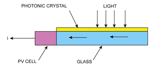
As shown in Fig. 1, a photonic crystal film of about 10µm thickness can be coated on a 3.2mm thick glass substrate which can laterally redirect light in different spectra. Different combinations of spectra can be made by suitably designing the photonic crystal. As the coating is thin enough, a transparent solar panel can be realised with a proper design where solar cells can be put on edges of the glass for electricity generation.
In a conventional Si PV cell, a lot of light energy is lost due to reflection. Conventional multistack dielectric antireflection coating may be used, which is costly and shows only limited bandwidth.
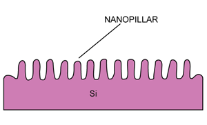
A maskless process requiring just a few steps has been developed to provide antireflectivity on silicon, which has low reflectivity over a wide acceptance angle. At a wide bandwidth of 400-800 nm, weighted reflectivity on silicon can be substantially reduced from 41 to 3 per cent at an acceptable angle of 15° and from 43 to 15 per cent at an acceptance angle of 60°. Fig. 2 shows such surface morphology on silicon with nanopillars providing low reflectivity over a wide acceptance angle.
[/stextbox]
[stextbox id=”info” caption=”2. High-brightness LEDs” bgcolor=”FFBAF6″]
Currently, high-brightness light-emitting diodes (LEDs) are the most promising light source, as these offer better efficiency, longer life and higher mechanical strength. Because high-brightness LEDs have a typical heat flux of over 100W/cm2, conventional packaging is not suitable. High junction temperature in LEDs substantially degrades the efficiency, colour quality, reliability and life of the solidstate lighting devices. Failure analysis always shows that the failure is not on the LED itself but on different package components due to high operating temperatures.
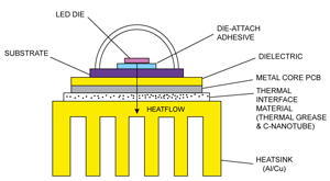
Nanomaterials can play a big role in heat dissipation in LEDs. As shown in Fig. 3, a die-attach adhesive not only attaches LED die to the substrate but also provides thermal and electrical conduction between the LED die and the package. Hence the heat-conducting ability of die-attach adhesive is very critical to the performance.
The existing epoxy adhesive has very low shelf temperature at -40 to -20°C, which is needed to lower the reactivity. This makes it very inconvenient and energy consuming to transport and store the material. Second, most of the epoxy resins need to be cured at a high temperature of above 130°C for a long time, which may damage the LED. The high curing temperature wastes energy and reduces mass production efficiency.
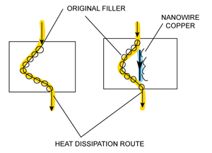
Research work in this area has led to the development of a die-attach adhesive with high thermal conductivity of about 25W/MK, low curing temperature of about 85°C and high shelf temperature of -10°C using nanomaterials and processing technology. This was made possible by using metal nanowires as filler additives in the adhesive matrix. These filler additives can fill the gaps between the original commercial fillers to form a continuous and multichannel heat transmission pathway to enhance the thermal conductivity as shown in Fig. 4.
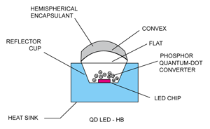
A series of low-cost environment-friendly (heavy-metal-free) luminescent quantum dots as the down-converting phosphors for high-performance LED devices has been developed. These luminescent, spectrally tunable quantum dots are coupled to a single-crystal LED chip to serve as a colour converter.
Quantum dots are quantised electronic structures in which electrons are confined with respect to motion in all three dimensions. Their properties resemble those of atoms in an electromagnetic cage, rendering possible fascinating novel devices. Typically, the size of a quantum dot is 10 nm and it may contain ten or more atoms. The size generally varies from 4 to 20 nm at room temperature depending on the type of the material. Such drastic reduction in size leads to carrier localisation in all three dimensions.
Using proper combination of quantum dots with different sizes and compositions and with improved package design, it is possible to manufacture high-quality, non-toxic white solidstate lighting devices with high colour rendering index (CRI>85) and high efficacy (>60 lm/W). Quantum-dot technology can significantly save energy and improve the colour quality of conventional LEDs.
There are two main classes of white LEDs: multi- and single-chip devices. Multichip white LEDs (RGB LEDs) constituted by red, green and blue emitting chips show three emission bands and possess a good CRI, good efficiency and well tunable colour. However, the efficiencies of red, green and blue LEDs change over time at different rates. Hence after a high-quality white light is produced initially, the quality of the white light degrades over time. Also, the cost of multichip white LEDs is high.
In comparison, single-chip white LEDs are low-cost and offer a high luminous efficiency, making them suitable for general-purpose lighting in the future. These LEDs are also called down-conversion LEDs, in which the blue light is downconverted into the light of a longer wavelength and the combination of blue and yellow lights is interpreted as white light by the human eye.
However, commercially available white LEDs emit a harsh and bluish cold-white light with poor colour rendering properties. This limits their wide-scale use in indoor illumination. When these white LEDs are used as the backlight of an LCD, the pale white light from blue and yellow hues cannot express the natural colours of objects faithfully in general circumstances.
Quantum dots can be easily optimised in size to a white light spectrum. The small size of quantum dots, which is much smaller than the wavelength of visible light, can also eliminate all light scattering and the associated optical losses. Thus highly luminescent and spectrally tunable quantum dots can be coupled to bright and efficient single-crystal LEDs. This approach utilises quantum dots as the downconverting medium, which efficiently absorbs blue light emitted by, for example, highly efficient gallium nitride LED and converts it into another wavelength of choice.
One of the most serious obstacles to using quantum-dot LEDs in consumer products is the toxicity of cadmium- and lead-based quantum dots. This problem has been addressed by developing high-luminescence, non-toxic quantum dots using InP/ZnS core shell.
First, nanoparticles of quantum dots using InP/ZnS with tunable size and colour are made. It is then followed by a wet chemical process to form a uniform inorganic protective shell on the quantum dots to achieve stability of the quantum dots and to improve the reliability of the polymer encapsulation of the LEDs. Then the encapsulated quantum dots with shells are further modified to make them well dispersed in the polymer matrix. The luminescent, spectrally-tunable quantum dots are then coupled with single-crystal LED chips to serve as a colour converter. Fig. 5 shows the scheme of a non-toxic quantum-dot LED.
[/stextbox]
[stextbox id=”info” caption=”3. Building materials” bgcolor=”FFC79C”]
In a typical office building, air-conditioning is the largest energy guzzler, which consumes about 48 per cent of the total energy. So the demand for better thermal insulation in the building enclosures has dramatically increased over the last few years.
To improve thermal insulation of composite wall panels, it is not practical to increase the wall thickness significantly. Research in this area is therefore focused on reducing the thermal conductivity of the wall materials without compromising on the other beneficial properties.
Introduction of porosity is the most straightforward way of improving thermal insulation. But porosity reduces structural strength and increases moisture uptake, which leads to corrosion. Nanomaterials and nanotechnology can address this issue. One solution is to use thermally insulating coating of aerogels and titanium dioxide (TiO2) nanoparticles on building materials like conventional glass, tiles and aluminium plates.
The high porosity of aerogels makes these an excellent thermal insulator. However, when radiation becomes a significant heat transfer mechanism at high temperature, the insulative performance of aerogels decreases since these are highly transparent in the 3-8µm wavelength region. With the addition of opacifiers, e.g., TiO2, this infrared transparency of aerogels can be reduced or even eliminated, ensuring that the insulative coating is suitable for a wide range of climates.
Another merit of nano TiO2 particles is their photo-induced superhydrophilicity property that can provide a self-cleaning function. This property makes these particles one of the most promising contenders for insulative coating in outdoor applications.
Another solution to reduce electricity consumption is use of high-performance cementitious materials for construction of the external wall with enhanced thermal insulation. For a given wall thickness, the thermal conductivity could be reduced if solid concrete is replaced with foamed concrete.
To meet the structural requirement, the foamed concrete should have compression strength equal to or greater than 30 MPa. For reducing the electrical consumption of the air-conditioning system, it should have thermal insulation property of less than 1W/mK. To achieve these technical requirements, lightweight sand and a foaming agent are used to make lightweight concrete with low thermal conductivity.
To maximise the strength, Pozzolans along with thermal curing is provided. Further, to prevent corrosion of steel reinforcement, a fibre-reinforced cementitious composite composition is applied to the wall surface. It acts as the barrier to water and chemical penetration. It has been found that by suitably adopting this technology electric power consumption of air-conditioning can be reduced by half.
[/stextbox]
[stextbox id=”info” caption=”4. Carbon-nanotube GHz amplifier” bgcolor=”BDBDBD”]
Carbon nanotube field-effect transistors (CNFETs) have been used recently to build a GHz amplifier. CNFETs are very attractive for future RF applications such as amplifiers, mixers and switches. Carbon nanotubes and graphene materials have superior electrical, mechanical strength and thermal properties, thanks to their one-dimensional transport and extremely strong carbon-carbon bonds leading to large mean free paths, high current densities and low thermal noise. Researchers are investigating ways of exploiting these characteristics to develop better performing electronic devices.
Ballistic transport of electrons through semiconducting carbon nanotubes has led to the development of CNFETs—one of the key building blocks of any electronic application. The one-dimensional tube structure allows quantum-capacitance limited operation, resulting in low input and feedback capacitance. It also significantly reduces the scattering probability, thus promising high-frequency performance with low figures. The structure also causes the drain current to be linearly dependent on the applied gate voltage, promising uniquely linear devices.
CNFETs are thermally robust, which simplifies the heat management. The current conventional semiconductor devices used in RF front-ends can be designed with high linearity but at the expense of reducing the operating efficiency to about 5 per cent. CNFETs recently developed deliver similar linearity but at 70 per cent less dissipated power. The system has deep impact on the battery life and reduction in heat dissipation.
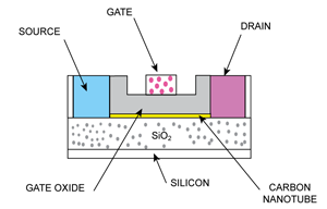
Typical construction steps are as follows: In a CNFET, thousands of carbon nanotubes are laid out between the drain and the source, providing a low resistance channel as shown in Fig. 6. The current flow through the channel is controlled by a top gate, separated from the tube array by a high-K dielectric. The base substrate is Si, which serves as the mechanical platform. A thick SiO2 is grown over it to minimise the device parasitics for high-performance operation. On this layer, a suitable catalyst is deposited to enhance growth and directionality. Then the carbon nanotubes are grown in a CVD furnace. Source and drain fingers and pads are then defined by the use of standard photolithography. Then a gate oxide is grown, on top of which the gate is patterned.
Source-to-drain distance, or channel width, is 0.8 µm. Gate length is about 0.45 µm and total gate periphery is 800 µm. The amplifier based on CNFET is typically biased at VGS=–0.5V and VDS=2.5V. Gate and drain DC bias are applied through choke. About 12.5 dB of gain can be obtained from a single stage centered at 1.3 GHz as shown in Fig. 7.

[/stextbox]
[stextbox id=”info” caption=”5. Carbon-nanotube pressure sensor” bgcolor=”FFEFD4″]
There has been much interest over the last couple of decades in exploiting the outstanding electrical, mechanical and optical properties of carbon nanotubes to fabricate micro-electromechanical system (MEMS) devices. In 2010, a carbon nanotube forest-based pressure sensor was developed that had a nearly symmetrical response for both positive and negative gauge pressures, using a suspended diaphragm entirely covered with CNT forest.
Achieving reliable devices based on individual CNTs with high repeatability is still very challenging, because of the structural variation between individual nanotubes. This problem can be addressed by using CNT forests—a macroscopic network of virtually self-aligned CNTs which have anisotropic electromechanical properties that can be used in many MEMS applications.
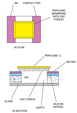
CNT forests provide a very large surface area and exhibit piezoresistivity when a lateral stress is applied. This property has been utilised to create a very sensitive and accurate physical sensor for pressure measurement. The sensor is fabricated by a deflectable, 8µm thick parylene—a biocompatible polymer membrane—and hence is of particular interest for medical applications.
The membrane is suspended by a silicon frame. The sensitivities to positive and negative gauge pressures are found to be comparable in magnitude with the average values of -986 and +816 ppm/kPa, respectively.
As shown in Fig. 8, multiwalled CNT forest is supported on a 5×5mm2 membrane of parylene-C of 8µm thickness. The two opposing ends of the forest are connected with the 130nm thick Mo metal pads on the substrate that are used to measure the resistance of the forest.
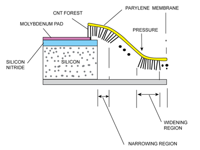
When pressure is applied to the membrane, a strain is generated in it as well as in the forest, leading to a change in the resistance of the forest due to its piezoresistive effect. The source of piezoresistive effect of the CNT forest is related to the change in distances between individual CNTs due to lateral strains applied to the forest.
As shown in Fig. 9, a positive pressure that deflects the membrane downwards can widen the CNT separation around the centre region of the membrane and increase the resistance in the region. However, it can also narrow the separation around the two border regions between the membrane and the substrate, thereby decreasing resistance in these regions. The opposite behaviour can be caused by a negative pressure.
The polarity may be determined by the collective piezoresistive effects across the forest including the two border regions. However, these border regions are relatively large and play the dominant role in the overall piezoresistive effect.
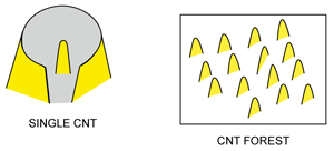
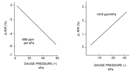
Fig. 10 shows the individual CNT and needle-like microstructure of the CNT forest. The fabrication process of the CNT forest starts with formation of a Si-nitride mask on both sides of a Si substrate, followed by patterning of a square window in the mask on the backside of the substrate. A molybdenum film is deposited with an electron beam evaporation technique to form the metal pads on the front side of the substrate. A catalyst layer made of 2nm Fe on 10nm Al2O3 is deposited in the region where the CNT forest will be grown.
Chemical vapour deposition technique is used to grow a forest of 400-600µm height using C2H4 as the carbon source, followed by deposition of 8µm thick parylene-C film binding the tops of individual CNTs. The backside window is made by dry etching of the silicon substrate. Fig. 11 shows the responses of the sensor for positive and negative gauge pressures.
[/stextbox]
