Engineers can take advantage of faster routing, improved workflow tools, and enhanced import/export capabilities, making it a practical choice for both hobbyists and professionals.
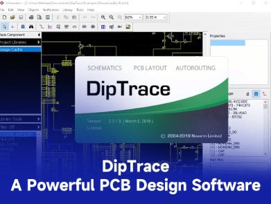
DipTrace is a comprehensive electronic design automation (EDA) software suite widely used for schematic capture and printed circuit board (PCB) design. Developed by Novarm Ltd., it helps engineers take an electronic concept from an initial circuit idea through to a manufacturable PCB layout all within a unified environment. Unlike simple drawing or layout utilities, it integrates multiple engineering modules: schematic editor, PCB layout editor with advanced routing tools, component and pattern editors, and real-time 3D visualization. This cohesive structure enables engineers to visualize, verify, and prepare designs efficiently for fabrication, reducing errors that often arise when using multiple disconnected tools.
One engineer put it well: “DipTrace lets me focus on the project itself instead of struggling with the software.” Its intuitive yet capable interface makes it suitable for designers ranging from hobbyists to seasoned professionals working on complex multi-layer boards. The tool’s real-time design rule checks and 3D previews help ensure layouts are electrically sound and mechanically compatible with enclosures before committing to fabrication.
The key features are:
It includes a broad set of capabilities that blend ease of use with engineering depth:

- Hierarchical and multi-sheet schematic capture for organized circuit representation.
- Advanced routing tools, including a shape-based autorouter and push-and-shove manual routing.
- Real-time design-rule checking (DRC) to catch spacing or connectivity errors early.
- High-speed and differential pair routing support for modern signal integrity requirements.
- 3D PCB preview and STEP export for mechanical verification.
- Extensive component libraries with easy custom footprint creation.
- Wide import/export compatibility, including formats like Gerber, IPC-2581C, and ODB++.
- Simulation workflows through SPICE integration for validating circuits.
Together, these features help engineers reduce design cycles, avoid costly revisions, and ensure boards are manufacturing-ready.
Open Source, Free, or Paid?
It is not open source. It is proprietary EDA software that offers both free and paid licensing options. The free edition called the FreeWare version is fully functional but limited in scale: designs are restricted to 300 pins, two signal layers, and one PCB per project. This makes it well-suited for students, hobbyists, and small prototype boards. Professional designers often find it a useful way to evaluate the tool before upgrading.
For more advanced requirements, it offers paid license tiers that remove those limits. Paid versions increase allowable pin counts and signal layers and unlock professional capabilities such as multi-board projects, full export formats (ODB++, IPC-2581C), team/enterprise collaboration functionality, and priority technical support. While pricing can vary based on region and edition, paid licenses are typically one-time purchases with optional upgrade plans rather than recurring subscriptions. The presence of clear tiers allows engineers to choose a license that matches project complexity and budget.
A common theme among reviews is appreciation for this flexible model: “It’s rare to get a free EDA tool that doesn’t feel intentionally crippled.”
What’s New?
The latest major update is DipTrace 5.2, officially released on September 17, 2025. This release builds on earlier milestones DipTrace 5.0 debuted on September 12, 2024, introducing major new capabilities like the enhanced Push and Shove Router and digital SPICE simulation; and DipTrace 5.1 arrived on November 19, 2024, delivering intermediate improvements and bug fixes.
The latest version focuses on workflow responsiveness and expanded interoperability:
- Walk Around Router modes and combined Push + Walk routing for more flexible trace placement.
- Automatic intermediate pad connections to reduce manual editing during routing.
- A more powerful Find tool that highlights and edits items directly from search results.
- Perimeter-only via stitching for cleaner copper fills.
- Import support for EasyEDA Pro and Pulsonix projects.
- CSV/TXT pin list import to speed part creation.
- Custom net-color highlighting for visual clarity.
One user noted this release’s impact: “The improvements in 5.2 feel like real workflow boosts, especially the enhanced routing flexibility.” These refinements help designers get more done with fewer clicks and less manual correction.
It is often praised for its friendly learning curve and practical routing tools. Reliable autorouting for medium-complexity boards is frequently highlighted as a time-saving element. “The autorouter is a real time-saver when boards get dense,” wrote one engineer, emphasizing how the feature cuts down manual effort.
At the same time, some users compare its capabilities with higher-end platforms and point out relative limitations. “It’s powerful but sometimes feels simpler than some modern alternatives,” commented one long-time electronics designer. These critiques typically focus on advanced automation or extensive documentation features areas where enterprise EDA tools often excel. Nonetheless, most agree that for its price point (especially with a generous free tier), it delivers excellent value for engineers.
It remains a versatile and cost-effective EDA solution, balancing ease of use with advanced PCB design capabilities. Its structured licensing ranging from a genuinely useful free version to flexible paid licenses allows users to scale their design capability as needed. With the latest release, the software continues to refine workflows and expand interoperability for modern engineering teams. Whether you’re prototyping small boards or tackling more complex multi-layer layouts, it deserves consideration as a practical tool in the PCB design toolkit.
For more information, click here.