
Electronics powers our world, but at what cost? Massive energy consumption, hazardous chemicals, and waste plague PCB and IC manufacturing. Can tech go green before it is too late?

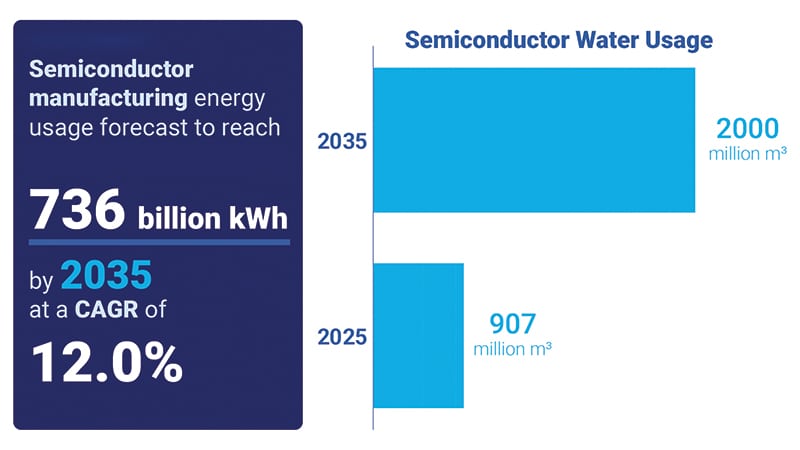
The manufacturing of printed circuit boards (PCBs) and integrated circuits (ICs) stands at the core of our tech-driven world but brings significant environmental concerns. In 2023 alone, Taiwan Semiconductor Manufacturing Company (TSMC), a leading industry player, used a staggering 25,000 gigawatt hours of energy and approximately 101 million cubic metres of water.

These figures highlight the immense resource consumption typical in semiconductor manufacturing, which involves millions of silicon wafers and hazardous chemicals. Given the current environmental challenges, how sustainable are these practices?
Table of Contents
PCB manufacturing mirrors these environmental concerns. The process heavily relies on chemicals such as ferric chloride and copper chloride, particularly during the etching phase. Moreover, the primary material used is Flame Retardant 4 (FR4), a type of epoxy resin derived from petroleum, underscoring the reliance on fossil fuels.
The procedure is notably wasteful, discarding about 70% of copper through subtractive methods. This not only wastes valuable resources but also significantly harms the environment. Have you considered the scale of waste generated by such processes?
Disposal poses another major issue. At the end of their life cycle, vast amounts of metals, plastics, and other materials from electronic devices often end up in landfills, leading to potential soil and water contamination. Some are incinerated to recover energy, which, unfortunately, contributes to air pollution.
However, there is a silver lining as the industry pursues improvements through operational efficiencies and sustainability goals. Techniques such as reducing manufacturing temperatures, streamlining process steps, and optimising chemical use are gaining traction.
Research into new materials that are potentially more sustainable or less harmful is also underway. Innovations in semiconductor materials, such as gallium nitride and silicon carbide, offer smaller chip sizes and lower emissions per chip.
Searching for Sustainable Solutions
IC manufacturers are focusing on developing new etching processes and photoresist materials. A key research area involves polyfluoroalkyl substances (PFAS), known for their robust carbon-fluorine bonds and resistance to atmospheric degradation.
While PFAS are effective in semiconductor production, they pose environmental risks due to their persistence and potential harm to wildlife and human health at high exposure levels.
The search for safer PFAS alternatives is ongoing, with the industry aiming to phase them out in applications such as PFAS photoresists by 2030. Notable successes include replacing hazardous substances like N-methylpyrrolidone in photolithography processes. Major chemical manufacturers introduced safer NMP-free solvents in 2021, and Taiwan Semiconductor Manufacturing Company (TSMC) adopted them in 2023.
Innovative strategies also involve modifying the molecular structure of etching chemicals. For instance, replacing tetrafluoromethane (CF4) with CF3I, which substitutes an iodine atom for a fluorine atom, weakens the strong carbon-fluorine bond, reducing the chemical’s environmental impact. Lam Research and Tokyo Electron are investing in these sustainable alternatives for dry etching and plasma processes.
These advancements are promising, but it remains to be seen whether the new chemicals can match the performance of traditional materials without compromising quality. Consumer demand and stricter regulations, such as the Eco-design for Sustainable Product Regulation in Europe and new global emissions standards, are crucial for adopting greener technologies. As these innovations progress, they help align electronics manufacturing with global sustainability goals.
| Bridging the sustainability gap |
| • Semiconductor giants lead the way. Industry leaders like TSMC, Intel, and Samsung are driving sustainability efforts, cutting emissions, reducing energy consumption, and optimising materials. Their initiatives set industry standards, aiming for meaningful environmental impact. • Contrasts in electronics manufacturing. While semiconductor leaders push sustainability, the broader electronics sector, particularly in Asia, shows mixed progress. Many manufacturers stick to cost-effective yet environmentally harmful processes. However, innovations like additive manufacturing for PCBs are emerging, offering a more sustainable alternative. • Opportunities in emerging markets. India, the US, and Europe are seeing significant semiconductor investments fueled by policies like the Chips Act. New plants incorporate energy-efficient tech and compact cleanroom designs, embedding sustainability from the outset and avoiding the limitations of older facilities. • Legislation and cost efficiency. Navigating regulations is crucial as governments tighten restrictions on toxic chemicals and mandate emissions reductions. The EU, Japan, and others enforce strict hazardous substance lists. Shifting to renewable energy and optimising energy and material use ensures compliance and cuts costs—simple measures like reducing rinse times and optimising standby modes boost both sustainability and profitability. • A call for industry-wide collaboration. Sustainable manufacturing requires more than just new technology—it demands a fundamental shift in mindset and operations. As new facilities rise, especially in India, the industry has a chance to embed sustainability from the ground up, setting new benchmarks for the future. |