


Despite its tangible benefits, microLED manufacturing is still too costly and full of challenges. But do the benefits outweigh the investments? If so, how soon can we expect them in displays?

Apple, Samsung, TCL and all the leading tech giants in the market have been announcing new products that have microLED (µLED) display screens. The industry is advancing with usage of µLEDs in ultra-large as well as small-size displays. From television sets and computer monitors to mobile screens, tablets, virtual reality, automotive displays, and smart wearables, all are being taken over. With benefits ranging from incredible picture quality and efficient lighting control to saving power, this emerging tech is tempting mainstream industries and innovators alike.

“Players pursue µLED displays because of their superior features. But that’s not the only major drive,” says Dr Xiaoxi He, Principal Analyst, IDTechEX, a market research firm. “The current LCD industry is mainly dominated by Mainland China. With South Korea taking the lead in organic light-emitting diodes (OLEDs), a new technology is being pushed to reshuffle the game in order to find new opportunities.”
While the term microLED refers to the size of the LEDs’ emitting area, there is no clear industry standard about the size that qualifies as micro. However, it is being used to define LEDs that range from 100µm per side or less. Without any doubt, new techniques and methods to manufacture such devices would be required.
Despite the innate potential and pursuit of display innovators, this flat technology has not culminated in mass production yet. Let us take a look at the potential uses of this technology and the hurdles being faced in their commercial production.


µLED benefits
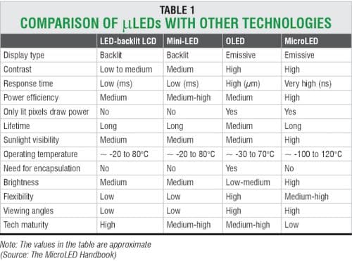
Experts believe µLEDs have good value propositions, such as colour gamut, high luminance, wide view angle, low power consumption, high dynamic range, high contrast, and transparency in comparison to other existing technologies. The ability to control each pixel for local dimming and brightening offers significant advantages.
Dr Xiaoxi explains that not all features are unique to µLED, some can be noticed in alternative technologies as well. “Some features are great, but they may not be realised by current technology capability, or may not be so important for some applications, such as those that require low power consumption.”
When the LEDs become very small, their external quantum efficiency (EQE) also drops significantly. For lighting, normal sized LEDs can offer low power consumption, but tiny ones may not—unless technology improves further. In addition, for applications such as signage displays, the power consumption is a less significant issue compared to wearables and AR/VR/MR. “Targeting applications addressing unique value propositions of µLED displays is very important,” explains Xiaoxi. Hence, the extent to which µLED displays can be beneficial depends on the required application, size, and other factors. Let’s have a look at a few.
In residential TV panels
South Korean and Chinese manufacturers are battling with announcements for new ultra-large residential displays. For instance, Samsung’s The Wall can max out from 2.8 metres (110 inches) to as big as 14.8 metres (583 inches) horizontally. The µLEDs bring superior colour purity and wider colour gamut than conventional LED displays. Its vibrant colours and deep black levels deliver intense contrast and immaculate detail for a one-of-a-kind visual experience.
The company says it can be sized as large as you want in 4K, or up to 7.4 metres (292 inches) in 8K, for an incredibly immersive viewing experience. In 8K, it can nearly be 15 times larger than a conventional 1.9-metre (75-inch) TV. Also, it claims to offer robust durability and energy efficiency with µLEDs that last for 100,000 hours.
µLED panels look similar to any of the existing regular LED and liquid crystal display (LCD), but the outcome differs significantly in terms of quality. The recently launched televisions come with thousands of µLEDs embedded in their back panel, but in a different arrangement with backlit techniques for efficient dimming control that produces a good contrast ratio. These do not have burn-out issues as in the case of earlier variants.
In your vehicle
Automotive market is benefiting from new applications of the emerging technology. The trend of developing automotive displays has reached another level where larger screens are made with higher resolution and high level of interactivity. Car manufacturers are now replacing the centre console with a touchscreen µLED display.
Typical vehicle displays for automobiles and spacecraft need central cluster panels and head-up display systems. This requires a technology with high reliability, sunlight readability and, most importantly, a wide working temperature. The µLEDs and mini LEDs show great advantage in luminance, lifetime, and robustness even in extreme weather. All the more, the head-up display systems need peak brightness that can be achieved with µLEDs.
In your accessories
Smart watches and eyewear with augmented reality/virtual reality (AR/VR) have been the goal of big players like Google and Apple. Many other companies across the globe are working on small µLED displays that can be fixed in these smart wearables, including headsets and wristbands.
Precisely, these displays require fast moving picture response time (MPRT) and low power consumption. The panels operated in bright rooms need a high luminant display, and µLEDs have proven to be the most efficient followed by OLEDs. TCL, a Chinese electronics firm, recently launched its new µLED-powered smart glasses.
µLEDs have also become a popular embellishment on functional applications like clothing or protective jackets for emergency service personnel. Their modular design of multiple same-size display panels teaming up to make a large-format screen, and their creative aspects of flexibility, high transparency, and ability to attach with sensors, make them a top choice for manufacturers.
For instance, a conventional mobile screen would not easily integrate with non-display components like touch, however a µLED can integrate many functional devices due to the considerable gap between each pixel inside the panel.
The big hurdle: Manufacturing
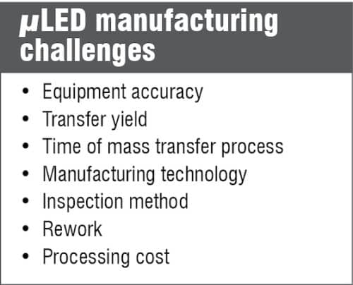
In spite of the huge number of applications, the process of manufacturing µLEDs is a lot more difficult than it sounds. µLED is simply an LED that converts electrical energy into light. But the extremely small µLEDs face numerous challenges in manufacturing as they require specific chip designs, manufacturing infrastructure, and assembly. Whether at wafer stage, post deposition, or at the assembling level, µLED makers need to have a reliable inspection.
“Traditionally the (LED) manufacturing process includes epitaxy and chip process, and it is the same for µLED. But higher performance is needed for the chip process. Mass transfer is another stage where we have no special equipment in the market,” says Falcon Liu, marketing director, PlayNitride, a manufacturing company in Taiwan.
First of all, the µLED epitaxy needs to be improved in terms of both wavelength and uniformity in thickness. The uniformity makes the wavelength more concentrated and thus can reduce the backend fine-tuning cost. But if the size is reduced to less than 100 micrometres, there can be power leakages due to non-uniformity while cutting around the chip.
The LED technology is not new but manufacturing a panel array with tiny components makes it challenging. µLEDs are microscopic versions of an LED without a package.
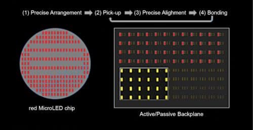
Imagine making a µLED TV panel. It may roughly require about 24 million individual µLEDs, which means manufacturing 24 million µLEDs and then transferring them to backplane of the TV. This mass transfer is the unresolved bottleneck for panel manufacturers.
One potential solution is the pick and place technique, even if it does not meet the ±1.5µm accuracy requirement. Flip chip technique is another one that is being widely followed, where a wafer carrying the LED layer is flip-bonded onto the driver circuit and soldered.
This method is, however, not quite feasible as only one substrate is flipped at a time, and there are high chances for pesky alignments and thermal mismatch.
Liu points out there are many ways of manufacturing for each application. He adds, “Production equipment is ready in the market, but needs modification. We need to find the correct process to improve yield and manufacturing time. Most of the equipment innovations are around mass transfer techniques. PlayNitride follows a stamping process, like pick up and place. “We produce Epi wafers by ourselves through a stamp to transfer µLED chips from wafer to backplane.”
“I think LED manufacturing is at a matured stage, but the manufacture of microchips needs careful understanding and effort. For µLEDs, the key is to make the manufacturing process rapid and massive. We need mass inspection and testing. A 4K display may need roughly 24 million µLEDs. It is not feasible to pick one by one,” says Liu.
He observes that manufacturers are concentrating on mass transferring to improve yield. “We are thinking on how to make it more efficient and perfect for mass production. We try to find new solutions, if it does not work, we keep innovating. Pick and place method is relatively mature. If there is something better, we move to it. New processes won’t be ready any time soon.”
Another alternative wafer production method is to etch the LED arrays for bonding to the circuit. While this method has less accuracy problems, it is very slow and also needs improvement to etch miniature LED components.
Fluid assembly technique, interpose, and self-assembly transfer are some of the trial and error methods that are widely practiced. However, the improvements to yield the desired level of transfer still needs exploration.
Not only are the initial stages of production difficult, the following stages of bonding add to the difficulty. The µLED chips are so small in size that the soldering paste may cause a short circuit. Inspection and testing stages also pose challenges due to the large number of chips, and hence manufacturers have to look for mass test methods to address it accurately. If a defective product is identified, the process of repairing it is much more complex. Currently, the µLED recovery solutions use UV irradiation rescue, laser rescue, and so on.
Supply chain and R&D focus
Currently, companies are relying on existing advantages of having complete mature supply chains for LED and display panels. The supply chains of µLEDs are a result of cross industry collaboration between electronic brands and leading edge technology players.
Apart from LED manufacturers, mini and µLED developers take help of mass transfer technology startups, semiconductor chip makers, panel makers, and production equipment suppliers. Display panel manufacturers, who are shifting their focus to mini and µLEDs, have also led more developers to step up R&D for new products.
In addition to panel manufacturers, LED producers have practically made it a goal to commercialise µLED and mini LED. The industry has noted an increase in the supply chain, especially in Taiwan and China where manufacturers like Epistar, PlayNitride, HC Semitek, and many others are working on developing mini and µLED technology. “There are definitely lots of technological challenges, and supply chain incompleteness. Therefore, targeting correct applications as the entry market is important,” suggests Dr Xiaoxi.
Inevitable price war
Liu tells that µLED is currently in the phase of exploring new opportunities, transparent displays, indoor ultra-large displays (like 100 or 200 inches), and applications in automotives. “The cost would be immense to compete with existing display technologies like LCD or OLED for now,” he adds.
The Taiwan government offers large subsidies to its domestic companies, encouraging mini and µLED development. Liu shares that even manufacturing associations have teamed up for innovations and funds to upscale production. “Government can support in promoting technology and import tax issues,” he adds.
Whatsoever, there is a concern whether the increase in capacity will lead to oversupply and price war. Industry sources opine that a large number of competitors may not be that bad. Such an increase in competitors is likely to expand the scale of the market, which in turn may lead to a breakthrough in innovations. Striking a balance between price and specifications becomes a necessity to meet affordability expectations of the market. The price war, however, could be inevitable for companies that focus on aggressive price strategy to stimulate and control demand.
Instead of worrying about the upcoming price war, mini and µLED developers should address technological barriers for market entry and come up with unique solutions to meet the needs of their prospective clients.
Yet to commercialise
Liu opines that more applications lead to commercialisation. “The primary market is display technology—ultra large displays. Meanwhile, with other applications demanding a lot of innovations, it may take around 4-5 years for the automotive industry, 2-3 years for the others to get commercial, and help to explore larger possibilities of adopting µLED tech in future.”
He adds that reducing the cost and number of defects while improving yield is the way to commercialise µLEDs. “Our research team has different challenges compared to mass production, yet innovations and trials can be achieved with experience.”
Despite the manufacturing struggles, innovators find µLEDs to be worth pursuing. Along with around 50% reduction in power consumption compared to OLEDs, these displays also offer longer lifespans. µLEDs do not exhibit burn issues, as in the case of OLEDs. Even so, many companies have failed to enter mass production and are far from reaching average consumers. The reduced cost of µLED and mini LED products and components will drive their adoption in the market. For the R&D engineers to achieve true design freedom, the primary problem of mass transfer and fast placement with accuracy has to be addressed first.
In conversation with EFY, Ron Mertens, CEO and founder of Metalgrass, a technology knowledge hub that is focussed on display technologies, says that commercialisation may take some time. “For µLEDs, there are many technical challenges in epitaxy, transfer, inspection/repair, full-colour displays, and more. The cost issue adds to it.”
He estimates that µLED adoption, which is likely to happen within two to five years, would begin mostly in three market segments—large-format TVs, micro-displays (for AR/VR), and perhaps simple wearables and automotive. “I think adopting this technology for applications such as smartphones, IT, TVs will take a longer time in the mass market. Even if these are just predictions, it is too early to call,” he adds.
However, to further materialise the µLED displays, innovators have targeted optimising manufacturing technology and reducing production cost. With an even tinier chip size, µLEDs require enhanced equipment and semiconductor-level equipment to process. Cooperation between the supply chains is pivotal for µLED chip manufacturing, mass transferring, testing, and repairing. Working with semiconductor material and equipment suppliers could be a feasible solution for µLED display production.
 Can µLEDs replace existing displays?
“They have the best performance, brightness, concept ratio, and are also reliable and flexible. A tech with immense potential, which is why we think it is disruptive,” says Liu. Indeed, µLEDs are an interesting technology with differentiating features.
While many companies do seem to be aggressively working on imbibing it in their new products, the heavy investments tend to push a few off the track. It might take some years for this emerging tech to become mainstream. Till then, the decision of investment depends on the application, and whether µLEDs can bring a greater benefit than incumbent technologies to the table.
Abbinaya Kuzhanthaivel is an Assistant Editor at EFY