Through-silicon vias. The most prominent technique for making true 3D chips today is by using through-silicon vias (TSVs). TSVs are vertical interconnects that link the many layers in a 3D IC. A TSV connects the two opposite sides of a silicon die or wafer. It runs from the front side of a wafer, typically connecting to one of the lower metal layers, all through the wafer and then out through the back.
TSVs are extremely thin and fragile and pose several challenges during fabrication. First, since the via goes through the active area and some of the metal layers, a large area around the TSV must be left free to avoid damages to the layers already deposited. Second, while manufacturing such chips, there is a risk of altering the threshold values of nearby transistors due to the stress applied to the silicon substrate. This could, in turn, alter the performance of the chip in unpredictable ways. Despite the challenges involved, TSVs are considered as the main option for the design and manufacture of 3D ICs.
2.5D. Semiconductor manufacturers such as Samsung and Xilinx have started using TSV technology in some of their chips, but the industry calls this slightly simpler version of 3D TSV usage as 2.5D. It is important here to define both 2.5D and 3D IC technologies. In 2.5D, one or several dies are mounted to another ‘inactive’ die with TSVs in order to route nets between the active die and the substrate. This technique involves the use of inter-posers, or electrical interface routing between two sockets or connections, to spread a connection to a wider pitch or to reroute a connection. A full 3D IC can be seen as one or several dies mounted to the backside of an ‘active’ silicon die through TSVs.
Xilinx, for example, uses a 2.5D technology called ‘stacked silicon interconnect’ in its new range of Virtex-7 field-programmable gate arrays (FPGAs). This method involves creating small dies and then putting several of them on a silicon interposer, instead of opting for huge dies which would not yield economic volumes. The Xilinx interposer consists of four layers of 65-micrometre metal on a silicon substrate. TSVs through the interposer allow this metal to be connected to the package substrate. Micro-bumps allow four FPGA dies to be flipped and connected to the interposer. The use of an interposer makes power distribution across the whole die simpler, and is believed to be the only 3D IC technology in high-volume production today.
While this technology may be applied to memories, FPGAs, micro-electromechanical devices and CMOS image sensors, experts feel it is not yet ready for application-specific integrated circuit applications. Once more design tools are available and the manufacturing and thermal management challenges in the use of TSVs overcome, we can expect to see full-3D ICs playing a huge role in the era of 20nm or smaller chips.

One must understand that 3D IC technology is not merely a stacking of components using vias instead of wires—if it was, it would go nowhere. Like the multi-core revolution, it requires new architectures and software.
The 3D IC technology has been talked about for the past eight years, but suddenly seems to be gaining momentum since last year. Global Foundries and Qualcomm announced a collaboration to work on 3D ICs in March 2010. Taiwan Semiconductor Manufacturing Company launched work on 3D IC design using interposer technologies in June. UMC, Pericom and Elpida made collaborative announcements concerning the development of DRAM/logic stacks. In September, Nokia declared that it would introduce a wide input/output (I/O) 3D inter-face in 2013. Xilinx launched Virtex-7 in October. Micron has suggested that it might be launching its hypercube in 12 to 18 months and Samsung is going big on wide I/O memory. In short, there is a lot of activity in TSV-based 3D IC technology space, and we hope to see some significant progress in the next two to three years.
Efforts to improve yield
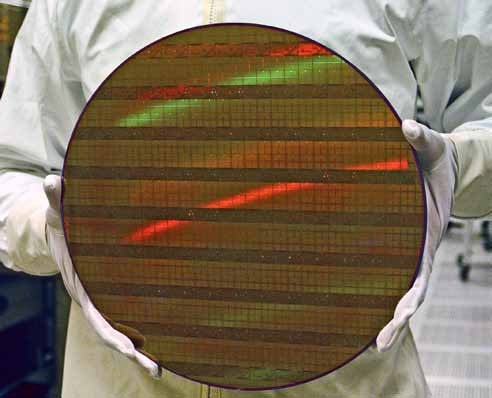
In the process of semiconductor fabrication, the proportion of devices on a wafer found to perform properly is referred to as the yield. Due to the complexity and sensitivity of the process and the components, there are many factors that reduce the yield of a semi-conductor fabrication process: Particle contamination, micro-scratching, wafer breakage, wafer misalignment, robot malfunctioning and even tool vibration due to environmental forces such as air flow. While these are general problems that have been haunting semiconductor fabs for years, newer yield-related problems have come about due to the reduced geometries. New techniques are emerging to conquer these problems.