


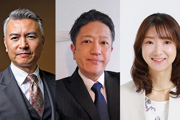
Think gold is just for jewellery? In semiconductors, it determines whether chips last or fail. At SEMICON India ’25, TANAKA PRECIOUS METALS leaders Yutaka Ito, Natalie Abe, and Satoshi Teshima share with EFY’s Akanksha Sondhi Gaur and Nidhi Agarwal how ultra-pure bonding wires and recycled metals are making materials smarter, supply chains stronger, and positioning India as a true architect in the global semiconductor mission.
Q. Can you outline your core offerings and expertise?
A. We provide a broad range of precious metal products, focusing mainly on electronics and semiconductors. Precious metals such as platinum, gold, silver, palladium,, iridium, and ruthenium, each chosen for their outstanding conductivity, reliability, and stability. These metals aren’t just shiny, they’re critical for everything from chip packaging to automotive electronics.

For the semiconductor market, we began by specialising in ultra-high-purity materials, such as gold wire with up to 99.99% purity, offering both superior electrical performance and long-term durability. Over the years, we didn’t stop at gold. We expanded into copper, palladium-coated copper, silver and aluminium wires, evolving into a global leader in bonding wire for semiconductor packaging.
Q. What are ultra-high-purity materials, and why are they essential in electronics?
A. When we talk about ultra-high-purity materials, we mean metals refined to an extraordinary level, often 99.99% pure or even higher, which experts call ‘four nines’ purity. This level of purity is critical for performance. Metals like gold, silver, platinum, and palladium need it to function properly in electronics. Even tiny impurities can create resistance, cause malfunctions, or shorten a device’s life. By keeping materials ultra-pure, semiconductors and miniaturised devices can run smoothly, reliably, and efficiently for years. Producing ultra-high-purity materials requires advanced technology such as melting, refining, and purity control, and this is one of TANAKA’s key areas of technical expertise.
Q. Why is the demand for these materials rising in advanced electronics?
A. Advanced packaging technologies such as fine-pitch wire bonding and high-frequency chip integration require clean surfaces and predictably conductive wires. Ultra-pure gold wires make this possible by allowing electrons to flow with minimal resistance.
For power electronics applications, thicker aluminium and copper wires or ribbon are employed. Their larger cross-section provides better current-carrying capacity and improved thermal robustness, which is essential for wide-bandgap devices such as silicon carbide (SiC) and gallium nitride (GaN).
Meanwhile, in advanced integration methods like chiplets, 2.5D/3D stacking, and heterogeneous packaging, traditional wire bonding plays a minor role. Instead, interconnect solutions rely on microbumps and hybrid bonding. Our silver adhesive paste provides a hybrid bonding solution for die-attachment and module-to-module heatsink integration, providing good heat dissipation with superior reliability under thermal cycling. These approaches help meet the demands for high bandwidth, reliability, and compatibility with diverse substrates.
Q. Have there been any breakthrough innovations in these materials in the past few years?
A. Bonding wire technologies are changing quickly to meet next-generation applications. Aluminium ribbon bonding wires are now used to handle higher currents and power, especially in electric vehicles and renewable energy systems. Copper wires, often coated with palladium, are becoming popular as a cost-effective and reliable choice for advanced power electronics. For materials like silicon carbide and gallium nitride, custom-coated or soft copper wires are being developed with customers to ensure better adhesion and long-term reliability. Sustainability is also shaping this field, with 100% recycled gold bonding wire now available through advanced recycling processes that maintain high purity while supporting greener electronics.
Q. When did TANAKA enter India, and how has the journey been since then?
A. We set up its sales and marketing office in Mumbai in 2019 with a team of about eight people focused on sales and customer support. While manufacturing is still done overseas, mainly in Japan, other parts of Asia, the India office supports electronics and semiconductor customers locally. The sector’s growth, especially after India’s semiconductor mission in 2023, has increased demand for materials like bonding wire and silver paste. TANAKA is now exploring feasibility studies and potential collaborations for local manufacturing to reduce import dependence and strengthen support for the Indian market.
Q. How large is the potential for advanced materials in India?
A. India’s semiconductor ecosystem is nascent but growing rapidly. Demand is expected to rise sharply, potentially surpassing China over time, though large-scale commercial production may start around 2026–2028.
Q. What is the global demand-supply situation for precious metals?
A. Post-COVID electronics growth and US-China geopolitical tensions are pushing companies to diversify sourcing. Europe is focusing on recycling and urban mining. The US is offering incentives for local semiconductor production. China continues to dominate refining but faces environmental scrutiny. With strong global demand and limited supply, recycling is becoming increasingly important.
Q. Who are the typical customers, and how do you approach the supply chain?
A. Customers include semiconductor fabs, OSATs, electronics OEMs (automotive, computing, AI, industrial automation), storage device makers, and e-waste recyclers. A resilient supply chain is essential to manage finite, high-cost metals, comply with regional regulations, and ensure product quality and traceability.
Q. Who makes decisions on materials and partners?
A. Material choices involve R&D and engineering teams (defining purity and mechanical properties), quality and operations managers (reliability, traceability, sustainability), and supply-chain officers (logistics, contracts, compliance). Often, end customers also specify materials for stringent reliability. In India, decisions are often aligned with global parent companies or design centres.
Q. What kind of partners or customers are sought?
A. Ideal partners have expertise in precious metals management, environmental compliance, recycling, and semiconductor technology. Collaboration spans OSAT companies, OEMs, and research institutions, especially where local regulations and waste management affect timelines.
Q. Are advanced materials sourced from India or globally?
A. Most materials are currently supplied from global manufacturing sites. We are presently exploring and assessing potential local partnerships for manufacturing or recycling, as the next step toward further expansion.
Q. Why do customers prefer Japanese suppliers?
A. Customers often prefer Japanese suppliers for their rigorous quality systems, process discipline, and continuous-improvement culture. At TANAKA, by combining over a century of metallurgy with a fully integrated value chain that includes mining, refining, manufacturing, R&D, marketing, and recycling, we ensure quality, reliability, and traceability.
Q. What stands out about your value chain?
A. The company manages the entire process from sourcing and refining metals to recycling, which ensures consistent quality. Recycling plays a key role as metals are recovered from industrial scrap and e-waste, then refined into high-purity components. This creates a closed-loop system that is trusted worldwide. Our long-standing leadership in bonding wires further strengthens this credibility.
Q. What innovations are being developed for advanced packaging?
A. Materials include gold, silver, copper (often palladium-coated), and aluminium wires for chip bonding and heat management. New trends focus on aluminium and copper wires for high-voltage/power electronics using substrates like silicon carbide and gallium nitride. Solutions are co-developed with customers to ensure adhesion, reliability, and performance.
Q. How does R&D and product customisation work?
A. R&D is collaborative, adjusting mechanical properties and purity to customer needs. Prototypes are co-developed, validated, and then scaled. Focus areas include softer copper for power devices, new alloys for next-gen substrates, and advanced recycling technology.
Q. What challenges are faced in India?
A. Regulatory approvals for environmental compliance and waste management are complex. Local partnerships are notable for secure and compliant manufacturing. A distributed global footprint helps mitigate risk during scale-up.
Q. Which policy changes could help?
A. Streamlined environmental and recycling permits, simplified import regulations for precious metals, and incentives for recycling infrastructure would strengthen India’s supply chain ecosystem.
Q. What is the talent situation in India?
A. Talent has not been a barrier; the India presence is market-driven. Hiring is from IITs and top institutions, with growing interest in semiconductors. Customers, however, are increasingly seeking qualified engineers for advanced materials, electronics manufacturing, and recycling.
Q. Should Indian academia develop specialised curricula?
A. Yes. Advanced programs in materials science, semiconductor manufacturing, recycling technology, and supply chain management will prepare students for electronics, sustainability, and global semiconductor roles.
Q. How are recycling and sustainability handled?
A. Two main streams are used: production scrap and urban mining from end-of-life products. Metals are recovered via advanced extraction methods, analysed for purity, and refined. Gold bonding wires can be produced entirely from recycled material, supporting sustainability and supply security.
Q. How has the business mix evolved?
A. The focus has shifted from traditional assets to high-tech industrial solutions. Currently, about 70% of revenue comes from electronics and industrial applications, including bonding wires, electrical contacts, and AI/data storage components. The vision is to expand industrial applications sustainably, supplying advanced materials for AI, automotive, and consumer devices.
Q. Final message for the electronics industry?
A. Precious metals are no longer just stores of value; they are critical enablers of advanced technology. Long-term partnerships, rigorous R&D, and sustainable practices will drive innovation and reliability in the semiconductor and electronics ecosystem.
