


The tool aims to ease the challenges of designing intricate 3D interconnects, offering engineers a way to handle multi-die systems more efficiently in AI data centre applications.
Keysight Technologies has introduced 3D Interconnect Designer, part of its EDA portfolio, to support the growing intricacy of chiplet and 3D IC packages. The software aims to streamline workflows that have traditionally relied on extensive manual optimization of transmission lines, solder balls and micro-bumps, all while maintaining signal and power integrity.

The solution is relevant for semiconductor packaging, high-performance computing, and complex PCB designs. The system’s electromagnetic-based simulations allow engineers to analyze interconnect behavior and assess compliance with emerging standards such as UCIe and BoW. By providing a structured approach to design and validation, the software can help reduce the number of design iterations and support tighter development timelines.
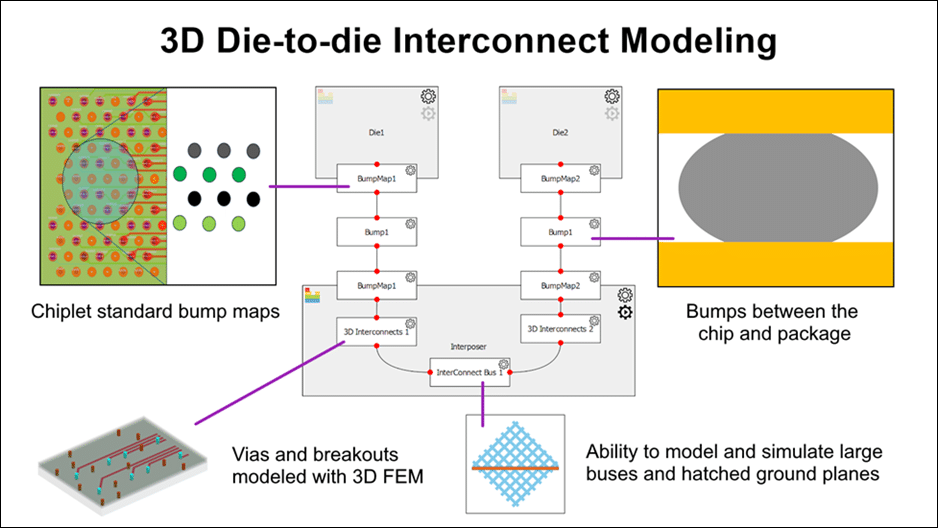
At the technical level, the environment can handle complex geometries, including hatched or waffled ground planes, which are often necessary in silicon interposers and bridges. It can operate as a standalone tool or integrate into existing EDA workflows. In combination with tools like Chiplet PHY Designer, teams can coordinate optimization across multi-die systems, focusing on accuracy and efficiency in dense, high-speed packages.
Key capabilities include automated handling of interconnect elements, early detection of potential signal and power integrity issues, and workflow management that helps maintain consistency across complex designs. The software does not eliminate all iteration, but it provides a structured framework to guide engineers through the process.
Nilesh Kamdar, EDA Design and Verification General Manager at Keysight, said, “With today’s complexity, manual 3D interconnect design and optimization have become a significant bottleneck. By streamlining the process and providing early insights into potential issues like signal and power integrity, we’re enabling engineers to get products to market faster and deliver compliant designs on tighter timelines.”