


What happens when transistor dimensions approach atomic limits? New chipmaking technologies are helping improve AI chip performance and efficiency.
Applied Materials has introduced three new semiconductor manufacturing systems designed to improve transistor performance and power efficiency at the 2nm node and beyond, addressing key challenges as the industry transitions to Gate-All-Around (GAA) transistor architectures for AI and high-performance computing chips.
The new technologies span deposition, etching, and materials modification processes that are increasingly important as semiconductor manufacturers push toward angstrom-scale process nodes. According to the company, the combined impact of these systems can contribute significantly to the performance and efficiency gains expected from future GAA-based chip generations.
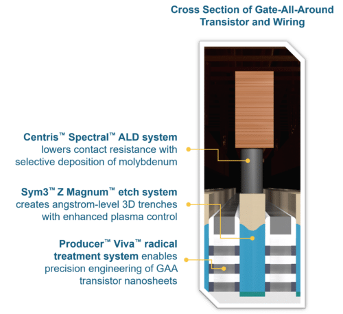
GAA transistors are becoming the industry standard for advanced logic devices because they provide better control of electrical current than previous transistor architectures. By surrounding the transistor channel on all sides, GAA designs enable higher performance while reducing power consumption, making them well suited for AI workloads and other compute-intensive applications. However, scaling these structures to smaller dimensions requires greater precision in materials engineering and manufacturing processes.
One of the newly introduced systems, the Producer Viva radical treatment platform, focuses on improving the surface quality of silicon nanosheets used as current-carrying channels in GAA transistors. Because electrical performance is highly sensitive to surface conditions at advanced nodes, even atomic-scale roughness or contamination can affect transistor behavior. The system uses ultra-pure neutral radicals to perform uniform surface treatments without causing material damage, helping improve electron mobility and transistor switching speed.
Applied Materials said the technology is already being adopted by leading logic chip manufacturers for 2nm and future process nodes. Beyond transistor fabrication, the system can also help reduce resistance in copper interconnects when combined with the company’s thermal annealing technologies.
The introduction of this systems reflects the growing importance of materials engineering in semiconductor scaling. As transistor dimensions approach atomic limits, advances in deposition, etching, and surface modification are becoming as critical as transistor design itself in delivering the next wave of performance and energy-efficiency improvements.
Click here for the original announcement.