


 Linear regulators like LM317, LM337, 78xx and 79xx, Zener diodes (1.3W) and reference diodes (e.g., LM336) are quite inexpensive and widely available. So you can use these liberally in power supplies. Here we design a universal power supply or a UPS using these.
Sometimes we need non-standard power supplies like ±11V, +9V and -3V. This circuit shows how to get adjustable or fixed dual power supplies using LM317, LM337, 78xx and 79xx. The outputs can be regulated from practically any level to the maximum voltages of the installed voltage regulators. And there is no need to use symmetrical regulators; you can use LM317 and 7809, LM317 and LM337, 7809 and 7909, or 7809 and7905, for instance.
As per application, the main difference between 78xx and 79xx and LM317 and LM337 is their quiescent (bias) current. The quiescent current for LM317 or LM337 is around 0.1mA. For the fixed regulators, 78xx or 79xx, the quiescent current can reach 8mA. So the difference can be up to 80 times.

This circuit can be built with 78xx and 79xx, or with LM317 and LM337, so you should calculate values of the associated components accordingly before use. (You can even mix these, like LM317 for the positive output and 7905 for the negative output.)
Universal power supply circuit
Fig. 1 shows the circuit of a universal dual regulator with LM317 and LM337. The idea is to have adjustable output voltage from a predetermined reference voltage. The positive output voltage V3 at CON3 (across points 1 and 2) is adjusted with potentiometer VR1. The negative output voltage V4 at CON3 (across points 2 and 3) is adjusted with potentiometer VR2.
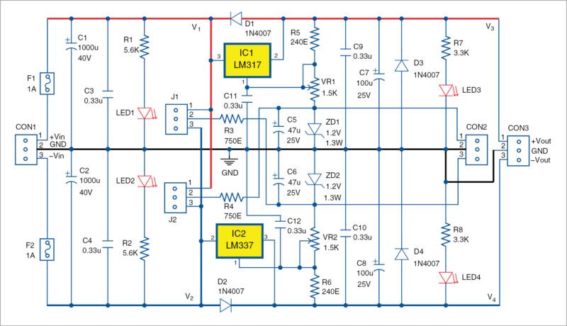
Regulators IC1 and IC2 should be mounted on appropriate heat-sinks having thermal resistance, preferably, below ten degrees centigrade per watt.
 You can use the circuit as a standard fixed power supply or as an adjustable power supply using 78xx and 79xx, or by using LM317 and LM337 with or without offset.
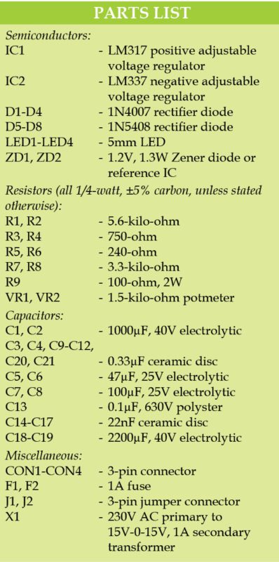
The components to determine before any application are: IC1, R4, ZD1, VR1 and R5 for the positive power supply and IC2, R3, ZD2, VR2 and R6 for the negative power supply. These components depend on the selected ICs and the required output voltage range. The minimal load current for the IC1 and IC2 should be respected in all cases.
Example 1
If you use LM317 as IC1, you can select R5 = 240-ohm, VR1 = 1.5-kilo-ohm and ZD1 reference diode for 1.2V. You will have regulation of the output voltage V3 (at point 1 of CON3) from ground up to around 8V. Fortunately, in most cases you can neglect the current of adjustment pin of LM317/LM337. In that case you will have:
Vout(positive) = V(LM317) x (1+VR1/R5) + Vref1
Vout(negative) = V(LM337) x (1+VR2/R6) + Vref2
V(LM317) = V(LM337) = 1.25V
Vref1 is from ZD1 and Vref2 is from ZD2. ZD1 and ZD2 can be the low-cost 1.3W Zener diodes with appropriate voltages. Also, instead of ZD1 and ZD2 you may use an IC (such as LM336 or TL431) for the reference voltages 1.2V, 2.5V, 5V, etc.
Jumpers J1 and J2 give the options to select positive and negative offsets for IC1 and IC2. In each case you should put the Zener diodes ZD1 and ZD2 in the desired direction. Offset outputs can be obtained at CON2.
Example 2
If you use 7805 as IC1, you can select R5 = 510-ohm, VR1= 510-ohm and ZD1 reference diode for 5.1V (such as 1N4733). You will have regulation of the output voltage V3 from around ground level to above 5V. So now you will have:
V3=Vout(positive) = V(78xx) x (1+VR1/R5) + Id x VR1 + Vref1
V4=Vout(negative) = V(79xx) x (1+VR2/R6) + Id x VR2 + Vref2
Here V(78xx) and V(79xx) are output voltages of the fixed regulator (xx denotes the number of the series, for example 7805 for 5V regulator). Id is the current (quiescent) from the ground pin (bias current) of the regulator 78xx or 79xx.
Preferably, you should have:
Id (R5, VR1) ≤ 5 x I(IC1)
Id (R6, VR2) ≤ 5 x I(IC2)
But you cannot expect that in most of the cases due to lot of power loss in R5, VR1, VR2 and R6.
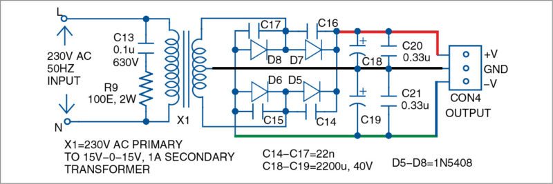
Input power supply. Fig. 2 shows the power section of the regulator with transformer and rectifiers. For a modular approach you should separate input power supply section from the regulator section. Then you can change one part of the power supply and keep the other intact. It helps in making different combinations with the rectifying and regulator sections.
Construction and testing
A single-side PCB pattern for universal power supply with LM317 and LM337 is shown in Fig. 3 and its component layout in Fig. 4. Single-side PCB pattern for the input power supply section is shown in Fig. 5 and its component layout in Fig. 6


Download PCB and Layout PDFs: click here
After assembling the circuit, connect the supply from CON4 to CON1. Now positive and negative outputs can be adjusted separately. Pin details of voltage regulators used in Fig. 1 are shown in Fig. 7.

ZD1 is for LM317, ZD2 is for LM337. Jumper 2 (J2) controls the applied voltage for the ZD1 and LM317. Jumper 1 (J1) controls the applied voltage for the lower Zener ZD2 and LM337.
When J1 is open and 1N4731 Zener is used (no shorting). ZD2 for LM337 operates as simple diode with voltage drop of around 0.7V. The forward current is only from VR2 and R6.
When J1 is shorted between points 1 and 2. ZD2 for LM337 operates as a simple Zener diode with voltage drop of around 4.3V. The current is from R3 and VR2.
When J1 is shorted between points 2 and 3. ZD2 for LM337 operates as a simple diode with voltage drop around 0.7V, but with higher forward current (compared to the case of no shorting).
Similarly, you can get various outputs by shorting J2 between points 1, 2 and 3.
Glowing of LED3 and LED4 indicates the output status of LM317 and LM337, respectively.
EFY note
- 79xx can replace LM337, and 78xx can replace LM317, in the same PCB with additional wiring. Please refer datasheets of both the ICs before making changes.
- We have not tested using LM78xx and LM79xx regulators, so the PCB shown here is designed for LM317 and LM337 only.
Feel interested? Check out other electronics projects.

Please make the Circuits section ad free
waht is the purpose of zener diodes?
what changes should i make to get 7v reguated voltage?
What is the use of zener
What is the minimum and maximum output voltage.
What is the correct place to connect Fuse in a transformer ?
In some projects, fuse is connected at primary side and some have secondary fuses. Also, some projects have fuses at primary side with ratings of secondary current ? Please explain these