


Should I use an FPGA or a microcontroller? This has always been a discussion for every new embedded project. It seems that FPGAs are going to rule the future because of their flexibility, increasingly better power efficiency and decreasing prices. Instead of programming a chip by telling it what to do, FPGAs allow you to tell a chip what to be. But if you are new to FPGAs, it can be a daunting task to decide where to start and collect all the tools to support your learning. Using this article as your guide, you can solve this problem by first selecting the vendor for the FPGA, then selecting an appropriate family of chips from the vendor and finally deciding a suitable development board.
We also explained the difference between an FPGA and a Microcontroller.

The first thing you need to settle yourself on is selecting a suitable vendor and family of FPGAs. The tool chain is one of the most important factors that will influence this decision. Though all manufacturers have a complete tool chain for each of their products but everyone will have a different opinion about the feel of different tool chains. So build your own opinion by downloading software tools from different manufacturers’ websites and play around with them. You can start working with these tools without any hardware required and get your designs at least up to the simulation stage.
Once you have decided on the software tool you like the most, you can go to the corresponding manufacturers’ websites (see table) to check out all the FPGA solutions they provide. By entering your design information in one of these software tools you can have an idea about the resources you need in the FPGA chip to implement it. This data will help you decide on the family and the size of the FPGA chip that you should use in your project.
Vendors normally break up their offerings into several families. You will need to go through their datasheets to figure out the most suitable chip for you. Below are some parameters that could help you decide on an FPGA chip:
1. On-chip RAM size
2. Input/output (I/O) interfaces
3. Number of DSPs/multiplier blocks
4. Device speed grade
5. Operating temperature
6. Package size
7. Device density
8. I/O pin counts
Again, the hardware description language (HDL) code will help you a lot here as the software tool can easily tell whether the code will fit into the selected device or not.
Selecting a development board
A development board is actually a printed circuit board (PCB) with some circuitry and hardware on-board to facilitate experimentation with a dedicated chip. These boards can save you from a lot of repetitive tasks. Imagine, you want to work on an FPGA-based project, but to be able to use an FPGA chip you need to solder this chip on the PCB as you cannot breadboard it. Also, you will have to set up a bunch of circuitry and hardware interfaces every time you want to work with that chip for different projects.
Obviously, this could frustrate you, especially when there are portions of the circuit which are going to be the same every time, such as the power supply. Also, there are lot of chances of soldering errors due to fine pitch of these ICs. Having most of the hardware and circuitry already set up makes life much easier and it is much more conducive to experimentation and general prototyping.
While choosing a development board, make a block diagram of your project and list out all the features you would need. FPGAs are ideal for use with high-speed peripherals and, in general, it is much easier to buy a board that contains the part you want, rather than trying to add one later on. For example, if you need a gigabit Ethernet, HDMI/DVI, PCI/PCI Express or external non-serial memory, you should buy a board that already has them as it will be very difficult to add them later on.
On the other hand, things such as MMC/SD cards, character LCDs, serial interfaces, LEDs and switches are easy to add and are not so much of a big deal to wire up. But it is better to get a board that has them so that you do not waste valuable time investigating failures caused due to soldering skills.
FPGAs are quite a complex device and, to build a project on a development board, it is important that you know how the interfaces and other hardware is wired on the board. Most manufacturers have proper legends on the board to indicate the interfaces but wiring sometimes can be difficult to trace. So check that the manufacturer provides complete schematic diagram, a reference manual, getting started guide, reference designs and sample codes.
There are many vendors selling development boards around FPGA chips from the manufacturers mentioned in the table. Below are some boards of different FPGA families:
Development boards for Xilinx chips Spartan-6
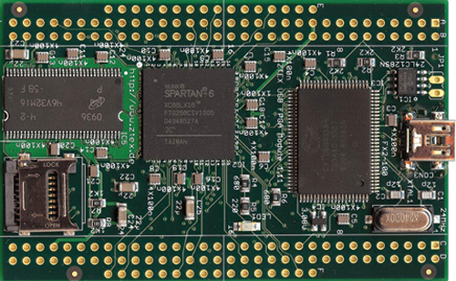
1. Digilent Nexys 3
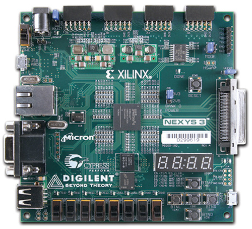
- 16MB Micron Cellular RAM
- 16MB Micron Parallel PCM
- 16MB Micron Quad-mode SPI PCM
- 10/100 SMSC LAN8710 PHY
- Digilent Adept USB port for power, programming and data transfers
- USB-UART
- Type-A USB host for mouse, keyboard or memory stick
- 8-bit VGA
- 100MHz fixed-frequency oscillator
- Eight slide switches, five push buttons, 4-digit seven-segment displays and eight LEDs
- Four double-wide Pmod connectors and one VHDC connector
- Rugged plastic case and USB cable included
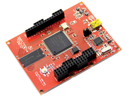
2. The Mojo
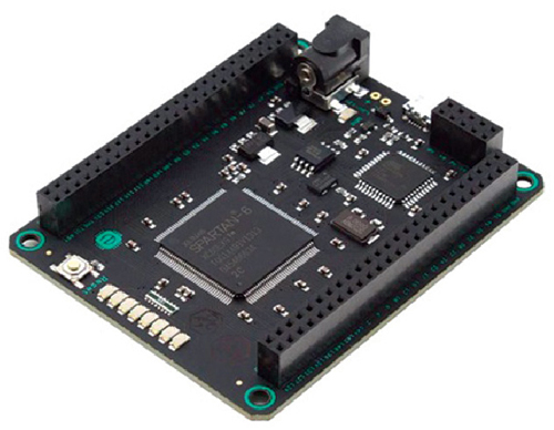
- Spartan 6 XC6SLX9 FPGA
- 84 digital I/O pins
- Eight analogue inputs
- Eight general-purpose LEDs
- One reset button
- One LED to show when the FPGA is correctly configured
- On-board voltage regulation that can handle 4.8V-12V
- A microcontroller (ATmega16U4) used for configuring the FPGA, USB communications and reading the analogue pins
- On-board Flash memory to store the FPGA configuration file
3. ZTEK USB FPGA module
- High-Speed (480Mbps) USB interface via mini-USB connector (B-type)
- Cypress CY7C68013A EZ-USB FX2 microcontroller
- Xilinx Spartan 6 LX9 to LX25 FPGA (XC6SLX9 to XC6SLX25)
- 90 general-purpose I/O’s (GPIOs)
- 15 special I/O’s (SIO)
- 64MB DDR SDRAM
- MicroSD socket for extensible Flash memory (standard and high-capacity (SDHC) cards, SPI mode support required)
- Bitstream loading from Flash to FPGA supported by the firmware
- Accessible from EZ-USB FX2, from FPGA and from host software using the SDK
- 128 kbit EEPROM memory (can be used to store the EZ-USB firmware)
- FPGA configuration/programming via USB using the EZ-USB FX2 SDK. (No JTAG adaptors or other additional utilities required)
- FPGA configuration/programming from Flash memory
ZTEK USB FPGA module has no on-board LEDs or buttons, but contains 64MB of SDRAM and a huge 90 GPIOs in a convenient plug-in module form factor, which is nice for dropping into a custom carrier board. Unfortunately, it does not have its own built-in power supply, so you need to place it onto the power supply or experimenter board, and then drop that onto your own board.
4. Avnet Spartan-6 Microboard
- Spartan-6 XC6SLX9-2CSG324C FPGA
- 64MB LPDDR SDRAM
- 128Mb multi-I/O SPI Flash
- 10/100 Ethernet PHY
- USB-to-UART port
- On-board USB JTAG circuitry
- Two Digilent Pmod compatible headers (2×6)
- Single-chip, 3-rail power with Power Good indicator
- Programmable clock chip
- Over-voltage and ESD protection on USB
- Four LEDs
- 4-bit DIP switch
- Reset and PROG push-buttons
Avnet Spartan-6 Microboard appears to be similar to the Arrow BeMicro. It is designed for embedded processor development and comes with a device locked SDK and ChipScope Pro licence, which is pretty good as these are quite expensive to buy separately. ChipScope alone is invaluable. I/O capability is pretty rudimentary with only two 8-bit PMOD connectors. The licenses are actually device locked to the XC6SLX9 (of any package), so it might be handy for you if you were developing your own board with this series.
5. Papilio Pro
- Spartan 6 LX9 FPGA
- High-efficiency LTC3419 step-down dual-voltage regulator
- Dual-channel FTDI FT2232 USB 2.0 full-speed interface
- 64Mb Micron MT48LC4M16 SDRAM
- 64Mb Macronix MX25L6445 SPI Flash
- 48 I/O pins arranged in a Papilio Wing form factor
- 32MHz crystal oscillator
Papilio Pro is a Spartan-6 LX9 board that retains compatibility with expansion wings made for the original Papilio. The design is released under a Creative Commons licence.
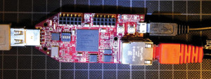
6. Pipistrello
- FPGA: Spartan-6 LX9, LX16, LX25 or LX45 in 324 BGA package
- Flash memory: 128 Mbit SPI Flash memory (Micron N25Q128A13ESE40G) wired for 1x, 2x or 4x wide data path
- On-board DRAM: 64MB (32Mx16) of LPDDR memory (Micron MT46H32M16LFBF-5) clocked at 200MHz (up to 800MB per second transfer rate) in 60 BGA package
- USB device interface: High-speed (480Mbps) interface using a 2-channel FTDI FT2232H chip. Channel A is wired for JTAG. Channel B is wired for serial or async FIFO mode.
- DVI/HDMI interface: Full HDMI interface (including I2C level translators for DDC) using a 19-pin HDMI type A connector
- Audio output: Two-channel audio output using 1-bit sigma-delta DAC
- Micro-SD card: Socket for micro-SD card, wired for SPI or native (4x wide) SD interface
- PMOD interface: Double-row PMOD connector that will allow the use of a wide range of PMOD devices
- LED indicators: Power (green), config state (yellow) and five user-defined LEDs
- User I/O: Papilio-style wing interface with 48 user-defined I/O signals. The boards have female headers installed on the wing interface.
Other than the ones mentioned above, the market is full of other popular boards for Spartan-6, such as XuLA2, 5I25 from Mesa Electronics, Numato Mimas, Numato Saturn and many more. XuLA2 has an LX25 chip on a small breadboardable PCB with built-in USB programmer, 32MB RAM, 8Mb Flash, 33 I/Os and SD card socket. The design is completely open source.
Mesa Electronics has a slightly baffling array of FPGA boards. Two interesting ones are 5I25, which is a PCI card with a Spartan-6 LX9, and 6I25 (PCI Express).
Numato Mimas provides a Spartan-6 LX9, 16Mb Flash, 100MHz oscillator, USB programming interface, eight LEDs, four switches and 70 I/Os.
Numato Saturn provides a Spartan-6 LX9, LX16, LX25 or LX45, 16Mb Flash, 100MHz oscillator, 512Mb LPDDR RAM, USB programming interface and GPIOs (via the FT2232H) and 118-150 I/Os.
Artix-7
1. Nexys-4
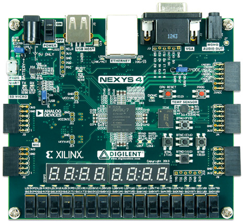
- 15,850 logic slices, each with four 6-input LUTs and eight flip-flops
- 4860 kbits of fast block RAM
- Six clock management tiles, each with phase-locked loop (PLL)
- 240 DSP slices
- Internal clock speeds exceeding 450MHz
- On-chip analogue-to-digital converter (XADC)
- 16 user switches, 16 user LEDs and two 4-digit seven-segment displays
- USB-UART bridge, 10/100 Ethernet PHY and 12-bit VGA output
- On-board 3-axis accelerometer, temperature sensor
- PWM audio output and PDM microphone
- Micro-SD card connector
- Digilent USB-JTAG port for FPGA programming and communication
Development boards for Lattice chips
1. Lattice XP2 Brevia
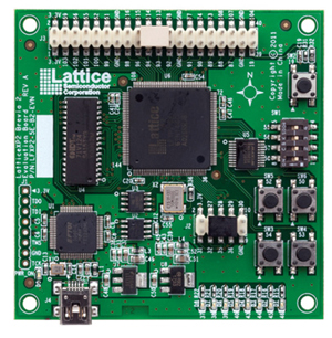
- LatticeXP2 FPGA: LFXP2-5E-6TN144C
- 2Mb SPI Flash memory
- 1Mb SRAM
- On-board USB controller for JTAG programming (FTDI -FT2232H)
- 2×20 and 2×5 expansion headers
- Push-buttons for GPIO and reset
- 4-bit DIP switch for user-defined inputs
- Eight status LEDs for user-defined outputs
LatticeXP2 Brevia is a development board with a small problem—the programmer needs a parallel port, and the USB programming cable is sold separately. The FPGA is a pretty low-end part as compared to the XC3S500E.
2. LatticeECP3 Versa
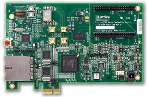
- LatticeECP3 FPGA: LFE3-35EA-8FN484C
- 64Mbit SPI Flash memory
- 1Gbit DDR3
- PCI Express x1 interface
- Four SMA connectors for electrical testing of one full-duplex SERDES channel
- Two RJ45 interfaces to 10/100/1000 Ethernet to GMII
- Expansion connectors for prototyping
- 14-segment alphanumeric display
- Switches, LEDs and displays for demo purposes
- Push-buttons for GPIO and reset, on-board reference clock sources
- Programmed using a mini-USB cable via PCROHS-compliant
LatticeECP3 Versa is one of the cheapest PCI-Express development boards so far. It also has two gigabit Ethernet ports and high-speed serial connectors. It appears that the FPGA device requires a licenced version of the design software.
3. Bugblat pif
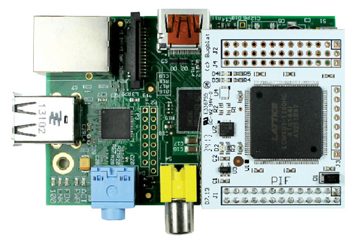
- A complete FPGA development target—FPGA programming hardware is not needed
- Plenty of on-chip 4-input LUTs—the pif-1200 has 1280, the pif-7000 has 6864
- Plenty of on-chip 9kbit SRAM blocks—the pif-1200 has 7, the pif-7000 has 26
- The FPGA is nonvolatile, with on-chip Flash memory for storing the configuration bit stream
- Up to 256kbits user Flash memory
- Hard-coded I2C, SPI, PLL and timer/counter blocks
- Powered from the Raspberry Pi expansion connector (P1)
- 47 pins of expansion connectors
- Red and green LEDs
- Support software supplied (in Python) for injecting a new configuration into the FPGA
- Example projects supplied, including a project that controls logic inside the FPGA from a web browser
Bugblat pif is a Raspberry Pi add-on board that provides a MachXO2-1200 or -7000, 17 external I/Os (in addition to those used to communicate with the Raspberry Pi), two LEDs and programming circuitry.
The other popular development boards for Lattice FPGAs are iCEblink40-HX1K Evaluation Kit, TRIFDEV and Bugblat tif.
iCEblink40-HX1K Evaluation Kit comes with a USB programmer, four LEDs, four capacitive touch buttons, configuration PROM, 68 digital I/Os and supposedly some PMOD and Arduino shield compatibility.
TRIFDEV is an Arduino shield that provides 58 extra I/Os, and can also be used as a standalone development board. It has a MachXO2-1200, USB programmer, two buttons and five LEDs.
Bugblat tif is a coin-sized, breadboardable MachXO2-1200 or -4000 board. It has ten I/Os, USB programming (with cross-platform open source software that does not require drivers) and two LEDs.
Development boards for Actel/Microsemi chips
1. Actel IGLOO nano starter kit
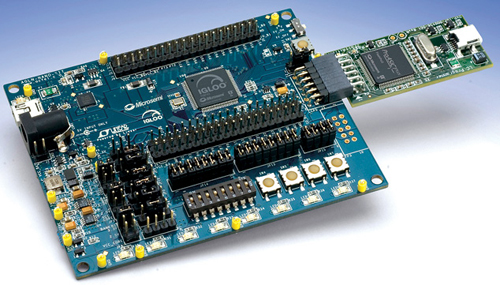
- Low-cost AGLN250-VQG100 device
- USB-to-UART connection for HyperTerminal on a PC
- A 20MHz system clock is provided using a low-power, precision oscillato
- Eight LEDs and four switches provide simple inputs and outputs to the system
- All I/Os available for quick connection to external circuitry
- Ability to switch VCORE from 1.2V – 1.5V
- Full current measurement capability of independent I/O banks and VCC for accurate power analysis
- Optional board power connector for an external supply, but none is needed when connected to a USB cable
- All components used on the board are low-power components, including LEDs (2 mA), resets (µA range) and oscillator (2-3 mA).
The other popular boards for Actel/Microsemi FPGA chips are Microsemi SmartFusion Evaluation Kit and TrioFlex ST32PA3-AP8.
Microsemi SmartFusion Evaluation Kit features an FPGA advertised as having 200k gates and an integrated 100MHz ARM Cortex-M3, 10/100 Ethernet PHY and on-chip MAC, USB-serial, on-board USB programming interface, OLED display, eight LEDs, two user switches and an indeterminate number of analogue and digital outputs.
TrioFlex ST32PA3-AP8 gives you an Actel A3P060 FPGA and 50MHz oscillator, with an AVR-compatible soft core preloaded in a stamp-sized module.
Development boards for Altera chips
1. DE0-Nano
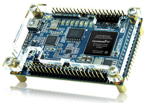
- Cyclone IV EP4CE22F17C6N with EPCS64 64Mbit serial configuration device
- Built-in USB-blaster cable for FPGA configuration
- 3-axis accelerometer with 13-bit resolution
- A/D converter, eight channels and 12-bit resolution
- Expansion headers (two 40-pin headers and one 26-pin headers)
- 2-pin external power header
- 32MB SDRAM
- 2kb EEPROM
- Eight green LEDs
- Four dip switches
- Two de-bounced push-button switches
2. Cyclone V GX Starter Kit
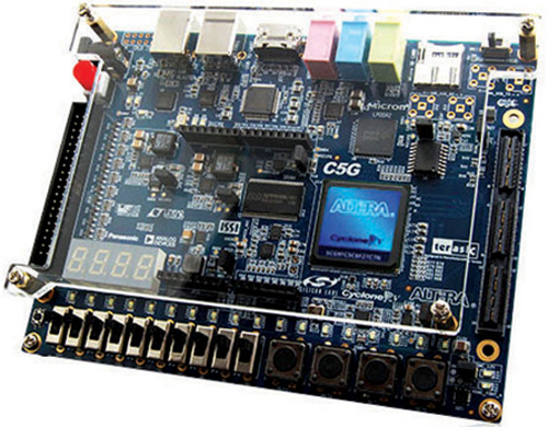
- Cyclone V GX 5CGXFC5C6F27C7N FPGA
- Configuration status and set-up elements
- High-speed mezzanine card (HSMC) x1, including 4-lane 3.125G transceiver
- 2×20 GPIO header
- Arduino header, including analogue pins
- SMA x4 (DNI), one-lane 3.125G transceiver
- 4Gb LPDDR2 x32 bits data bus
- 4Mb SRAM x16 bits data bus
- High-definition multimedia interface (HDMI) transmitter (TX), compatible with DVI v1.0 and HDCP v1.4
- 24-bit CODEC, line-in, line-out and microphone-in jacks
- Switches, buttons, LED and seven-segment displays
- Micro-SD card socket
- Provides SPI and 4-bit SD mode for SD card access
3. Arrow BeMicro
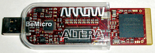
- Altera Cyclone III FPGA—
- EP3C16F256C8N
- Altera Nios II embedded processor
- 16MHz clock oscillator
- Three status LEDs
- Eight user LEDs
- 80-pin edge connector
Arrows’ BeMicro is small but you would need the corresponding protoboard to use any of the I/Os. It is mainly intended for embedded processor development. Another board from Arrow is BeMicro SDK, which is a newer version of the BeMicro that is intended for use with the Altera Nios II processor. It includes a Cyclone IV FPGA, microSD, 10/100 Ethernet, temperature sensor, 512Mb mobile DDR, integrated programmer, eight LEDs, buttons and switches and an 80-pin edge connector. A corresponding protoboard is also available.
As Altera is equally popular as Xilinx, you will find a lot of other development boards in the market such as Terasic Altera DE0, thin-layer embedded helix_4, KNJN Pluto boards, FTDI Morph-IC-II, Wayengineer boards and Amani F2. Each board is good for something or the other but you need to decide based on your project needs. Brief of each board is described below:
Thin-layer embedded helix_4. It is a Cyclone IV module designed by an Australian company that combines 4Mb of SRAM, 512Mb of DDR2 (in the larger model), Flash and a cryptography chip in a module that is designed to be mounted directly on your own PCBs. Carrier boards compatible with Arduino shields with USB programming via a PSoC are also available.
Terasic Altera DE0. The board looks comparable to Digilent’s Nexys2, though the connectors are not suitable for high-speed use.
KNJN Pluto. These boards are cheap and small. No on-board peripherals, so they seem more suited to dropping into a larger project than as a standalone development tool.
FTDI Morph-IC-II. This board combines a Cyclone II with an FT2232H USB interface chip to provide high-speed data transfer. It has a total of 80 to 96 I/Os split between the FPGA and FT2232H.
Wayengineer. Wayengineer sells a large range of very cheap Cyclone II boards from Shenzhen, mostly with RAM and a variety of I/O including LCDs, seven-segment LEDs, VGA and switches. Again, they are of great value if you already have some experience with FPGAs, are comfortable reading schematics and do not require any vendor support.
Amani F2. It has a Cyclone II EP2C5 with 4608 LEs on an Arduino shield. It provides 74 digital I/Os, including two PMod interfaces, a JTAG port, a push button and an LED. A pad is provided for an EPCS1 Flash memory device.
Development boards for Cypress chips
The major boards for Cypress FPGA chips are PSoC 4 Pioneer, freeSoC and freeSoC Mini. PSoC 4 Pioneer is Cypress’ own cheap development board. It has a PSoC 4200, which has a Cortex-M0 and supports for both Arduino shields and Digilent PMods, a CapSense slider, RGB LED and one button. freeSoC and freeSoC Mini are not FPGA boards, but rather are boards based on the Cypress PSoC, which incorporates an ARM Cortex-M3 and reconfigurable mixed-signal logic.
The author is a technical editor at EFY
