
We are all familiar with Arduino shields available in the market. These allow us to increase the functions and capabilities of Arduino boards. Without these it is difficult to connect the circuit to an Arduino board.
Generally, we use jumper wires for connecting an Arduino board to a circuit assembled on a breadboard. Management of cable connections and troubleshooting becomes very difficult while using jumper wires.
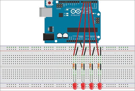
Most people find it difficult to design an Arduino shield using conventional or professional printed circuit board (PCB) designing software since these require typical measurements of Arduino for matching connector locations. Fig. 1 shows the interfacing of a circuit assembled on a breadboard to an Arduino Board.

We can easily make Arduino shields using Fritzing software. It is easy to use as compared to other software because here we do not have to provide any dimension details or alignment for proper placement of the connectors that are used to connect the shield with Arduino.
Fritzing is an open source software initiative that supports designers and artists who are ready to move from physical prototyping to the actual product. It was developed at University of Applied Sciences of Potsdam, Germany. The software allows designers, artists, researchers or hobbyists to document their Arduino based prototypes and create PCB layouts for manufacturing. The associated website helps users share and discuss drafts and experiences as well as reduce manufacturing costs.

Fritzing can be seen as an electronic design automation (EDA) tool for non-engineers. It has a code-view option, where one can modify code and upload it directly to an Arduino device.
There is a huge library in Fritzing to help us make shields for different Arduino and Raspberry Pi boards. We can get the artwork by simply making the schematic, which can be further adjusted in Arduino shield form. There are many routing options available in the software. In this article, we explain the making of an Arduino shield using Fritzing version 0.91 for Arduino UNO R3 for a single-sided PCB.
Steps for making an Arduino shield using Fritzing are:
1. Download Fritzing. The downloaded file can be used directly; you need not install it.
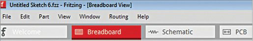
2. Go to Breadboard as shown in Fig. 2. Draw a proper connection diagram of the desired circuit using the component library in the software. Cross-check the connections in the software.
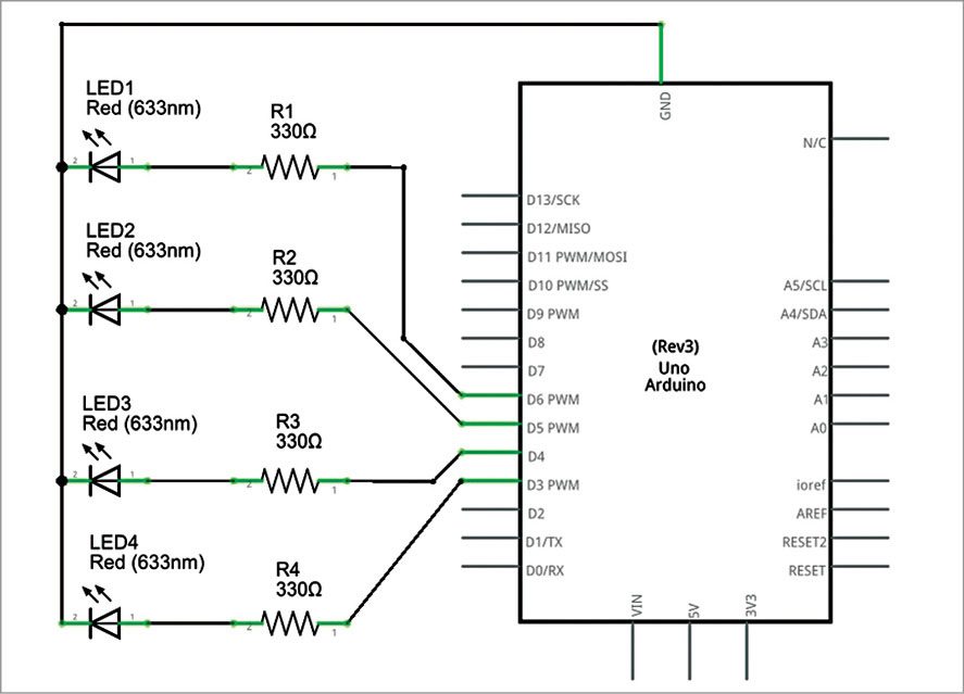
3. Go to Schematic and check if the connections are done in Breadboard. We can directly design a circuit in Schematic. For those who are new to designing of schematics, the option of Breadboard is recommended. The schematic made using Fritzing is shown in Fig. 3.
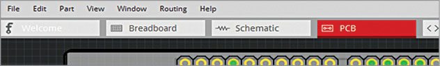
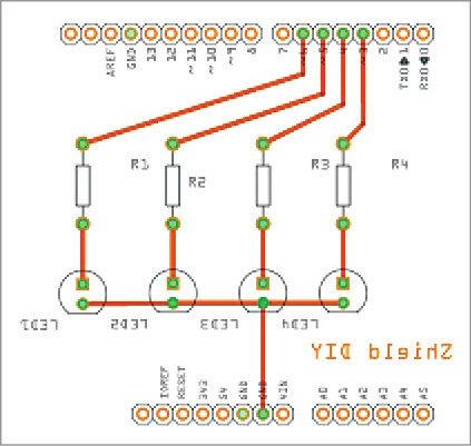
4. Go to PCB section of Fritzing as shown in Fig. 4. Select the type of PCB you need to make. Various options are available like Auto Routing and Layers Selection.
5. Select the settings for Copper Layer as per requirement. Route connections manually as per the circuit and the requirement. Fig. 5 shows Arduino shield PCB after routing. The settings are different for double- and single-side PCBs.
PCB
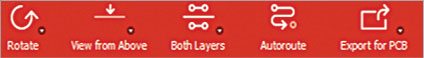
6. After preparing the PCB and proper routing of the circuit, click Export for PCB as shown in Fig. 6 and save the files in PDF format in the destination folder.
option after proper routing
7. Check the design rules by clicking Routing under PCB section.
8. If copper fill is required, it can be applied to the PCB using the relevant option under Routing options.
9. Place the berg strips/headers used for connecting the shield to Arduino UNO board on the same side for soldering on a single-side PCB. Careful soldering is required for this purpose. Since the berg strip header and routing tracks are on the same side, remove the plastic sheath from the berg strip before soldering. Place the sheath back after soldering. A long header of 25mm is recommended. Placement of the same is shown in Fig. 7.
10. Specify the type of file in which you are exporting the circuit diagram PCB artwork. If you export in PDF format, specify the folder where you want to save the exported file. A number of files will be saved in the target folder in PDF format for bottom-layer copper, top-layer copper, mask top, mask bottom, silk top, silk bottom and so on, and their respective mirror image files will be saved in another PDF file. We can easily select the desired file for a particular requirement.
11. Transfer the artwork on the PCB, which is cut to the required size. Proceed for etching and soldering of components.
Component images are distributed under CC-BY-SA, which will also be the licence for any generated breadboard views.
Download source code: click here
Madhuram Mishra is a student of ME digital communication at NITTTR, Bhopal
The article was first published on this website on 17th Feb 2016.