Graphene has long promised new sensors and electronics. The real challenge was not performance, but manufacturing. That bottleneck is now starting to break.
Graphene transistors promise faster sensing and new electronic functions. But most ways of making them do not scale well. Many processes grow graphene on one surface and then move it onto silicon. This transfer step often adds metal contamination, hurts performance, and makes it hard to use existing semiconductor fabs. Because of this, graphene devices have mostly stayed in labs or small pilot runs.
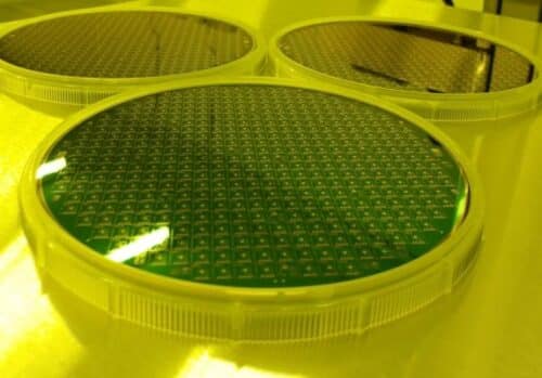
Paragraf, a UK based company addresses this by growing graphene directly on silicon. This removes the transfer step and keeps the process cleaner. It also fits better with standard semiconductor tools. The company has now shown this approach on a full 6 inch silicon wafer at its manufacturing site in Huntingdon. On this wafer, it built graphene field effect transistors using its own direct growth process.
Wafer size is a real bottleneck for companies trying to move from prototypes to real products. Until now, Paragraf made these devices on 2 inch sapphire wafers. That works for early testing, but it limits volume, uniformity, and cost control. A 6 inch silicon wafer fits much better into existing chip production lines and supports higher yields.
By moving to larger silicon wafers, the company is solving a practical problem for customers who want graphene devices they can actually manufacture and use. This includes teams building advanced sensors and electronic components that need stable performance, clean materials, and a clear path to scale.
The shift from small sapphire wafers to 6 inch silicon is not about a single breakthrough moment. It is about removing the barriers that have kept graphene from wider use. It brings graphene electronics closer to the processes, costs, and reliability that the semiconductor industry already relies on.
“This first 6-inch wafer out of our Huntingdon facility is a landmark moment for Paragraf,” said Simon Thomas, Co-Founder and CEO of Paragraf. “It demonstrates both the maturity of our graphene growth technology and our ability to scale it on industry-relevant substrates, while maintaining the contamination-free advantages of our approach required by many applications and customers.”