Single-chip device fuses sensing, memory, and AI for faster edge vision.
A new semiconductor breakthrough could reshape how smart cameras are designed, collapsing multiple electronic subsystems into a single diode and enabling faster, more efficient machine vision at the edge.

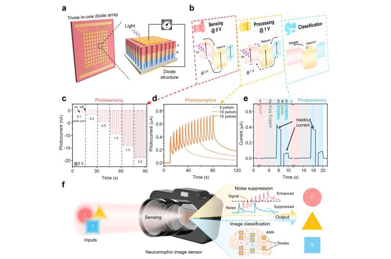
Researchers have developed a “three-in-one” diode that integrates image sensing, memory storage, and signal processing within a single electronic component. Unlike conventional camera systems—which rely on separate chips for capturing, storing, and analysing images—this device performs all three functions simultaneously on-chip.
At the core of the innovation is a layered aluminium gallium nitride structure that can trap and release electrons generated by incoming light. By adjusting voltage, the same diode dynamically switches between three modes: a self-powered photodetector, a noise-filtering photosynapse, and a multistate memory element capable of storing image data.
This architecture enables real-time image sensing while suppressing noise and retaining data locally—eliminating the need for separate processing hardware. In testing, arrays built from these diodes achieved over 95% accuracy in image recognition tasks, even when input images were degraded by background noise.
The design also introduces multi-level memory behaviour, with each diode supporting eight distinct electrical states. This allows the system to encode and process visual information directly within the sensor layer, a key step toward neuromorphic and in-memory computing architectures for imaging.
From an electronics perspective, the approach aligns with broader industry trends toward AIoT systems that demand compact, low-power, and highly integrated components. By reducing data movement between chips, the diode-based architecture could significantly cut energy consumption and latency in edge devices such as autonomous robots, surveillance systems, and wearable cameras.
The development signals a shift from traditional CMOS-based imaging pipelines toward compute-in-sensor electronics, where intelligence is embedded directly at the pixel level. If scaled commercially, such devices could redefine camera hardware by replacing multi-chip modules with single-component solutions optimised for real-time AI vision.