


A breakthrough chip built with next generation lithography could reshape how millions of quantum bits are manufactured reliably at industrial scale.
imec has announced the development of what it describes as the world’s first quantum dot qubit device fabricated using High Numerical Aperture Extreme Ultraviolet (High NA EUV) lithography. Presented during ITF World, the achievement marks a significant milestone in the effort to industrialize quantum computing hardware using advanced semiconductor manufacturing technologies already being developed for future AI and high performance computing chips.

The research addresses one of the biggest challenges facing quantum computing today: scalability. While quantum systems have shown promise in solving complex computational problems beyond the reach of classical computers, building a practical machine requires millions of reliable and interconnected qubits. Imec’s work focuses on silicon quantum dot spin qubits, often referred to as “industry qubits” because they can be fabricated using CMOS compatible semiconductor processes already widely used in modern chip manufacturing. This compatibility could eventually allow quantum hardware to benefit from decades of semiconductor scaling infrastructure and manufacturing expertise.
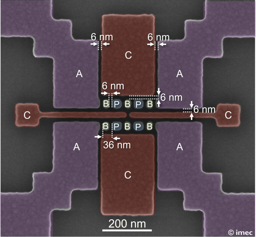
One of the major advantages of the new approach is the use of High NA EUV lithography to create extremely small and precise structures required for stable qubit operation. The researchers successfully fabricated functioning qubit networks with gaps as small as 6 nanometers between control electrodes. Reducing these gaps improves coupling strength between neighboring quantum dots while minimizing environmental noise that can destabilize quantum information. According to the team, the nanoscale dimensions could theoretically enable millions of qubits to be integrated onto a single chip.
Beyond miniaturization, the work also demonstrates progress toward reproducible 300 mm wafer compatible quantum manufacturing rather than isolated laboratory prototypes. Sofie Beyne, project leader and quantum integration engineer at imec, says, “We can leverage decades of semiconductor innovation and reuse the entire ecosystem of silicon scaling, moving quantum devices beyond lab experiments to large scale, manufacturable systems.”
