


The process of circuit design can range from developing a small toy to a large space station. Other applications may also include entertainment, defence, communications, medical, automotive, automation and so on, which involve logic, memory, control and decision-making. Designers have to simply identify the input and the required output.
Solutions for various problems and demands need to identify the basic requirements of circuit design. Designing a complex circuit starts with the process of investment, identifying product development challenges and design life cycle, and considering the return on investment.

Designing a complex circuit is one aspect of the challenge, whereas transforming the circuit design into a PCB Design is another. This design has to transform well into a physical form for the desired electric circuit to take shape.
A perfectly developed PCB Design is always a key to success in the manufacturing process while a poorly designed PCB leads to a waste of time and effort, rework and product failure. Worse, it may end up being useless and whose outcome does not correlate well with real-world scenarios.
So, besides having knowledge related to the positioning of hundreds and thousands of components and traces that meet physical and electrical requirements, a PCB designer must also have good knowledge of the manufacturing process.
A PCB designer has to follow the standards related to Design for assembly (DFA) while designing a PCB. These standards refer to the cost and efficiency of that product and offer minimum risk, clarity and simplification. Even assembler capability is important for getting an overall picture of the DFA.
Table of Contents
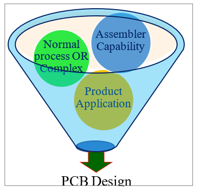
Substrate material FR4 is quite commonly used for creating normal and complex PCB designs, while polyamide material is used for high-speed RF capability designs.
When determining the choice of substrate material, a designer must have a strong understanding of the environmental conditions, which the PCB assembly can withstand.
Complex PCB designs might have some special assembly requirements such as mechanical component assembly, press-fit parts, adhesives, wire harnesses, enclosure assemblies, wire harnessing and test points.
Hence, the designer must consider all these so that the component placement details can be organised accordingly.
Complex PCB design requires some additional complex processes with respect to Via-in-Pad ( for fine pitch parts µBGA), wire bonding, wave soldering, onboard IC programming, conformal coating, surface finish etc. Such requirements are not applicable to a normal PCB design.
Also Check: High SpeedPCb Design Guide
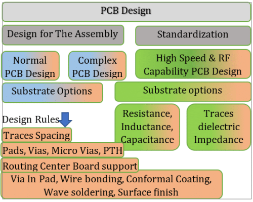
Design concepts are the same for all PCB design processes, but they differ for high-speed RF capability as these designs must consider resistance, inductance and capacitance as well as traces and dielectrics that affect signal raise times and impedance that limit the upper frequency.
Similarly, PCB design rules for the wave soldering process differ in designing component orientation and pad shapes. Getting the right pad shapes are the main concern for fine-pitch surface mount parts, while shadowing is the main concern for part orientation.
The reason for creating double-sided PCBs is so that the placement of complex components such as BGA, CSP, QFP, and DFN POP on the top side does not come in direct contact with waves. If unavoidable, then the package should be rotated 45 degrees relative to the direction of travel of the wave.
Also Check: IC Package Types Explained
Standards and specifications for PCB design performance and accessibility include IPC-2221, IPC-6011 and IPC-6012. Many PCB design software applications (PCB layout SW) are available as Windows-based packages such as CAD SOFT, Eagle PCB, Novarm’s DipTrace etc.
Introduction
While the term “Printed Circuit Board” is the most commonly used, it can also be referred to as “Printed Wiring Boards” or “Printed Wiring Cards”. The first PCB Design patent was developed in 1903.
Application of single and double-sided boards continued as non-plated through-hole till 1946. Further, in 1947, double-sided plate through-holes were developed and from 1960 onwards multilayer process was developed.
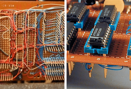
Before the advent of the PCB, circuits were constructed through a laborious process of point-to-point wiring. This led to frequent failures at wire junctions and short circuits when wire insulation began to age and crack.
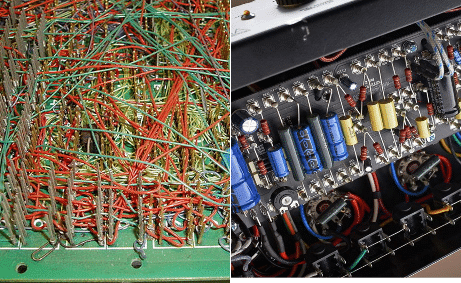
A significant advancement was the development of wire wrapping where a small gauge wire was literally wrapped around each connection point, creating a gas-tight connection, which was highly durable and easily changeable. This technique was the only option before the PCB was born.
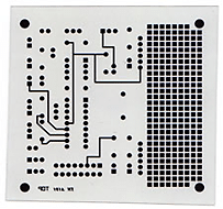
Printed Circuit Board
It is a board base for physically supporting and wiring the electronic, electrical and mechanical components. Mechanical support for components is provided by the board base, which is electrically connected through conductive traces and pads.
The board consists of substrates with copper tracks that act as wires to which components are connected. These components are soldered onto the PCB so that they are strongly held. Insulating and copper layers on the board contain signal traces for the power supply and ground.
Traditionally, components were mounted on the top layer in holes, which extended through all layers. These later came to be referred to as through-hole components. With the near-universal adoption of surface mount components, one can commonly find components mounted on both the top and bottom layers of a printed circuit board.
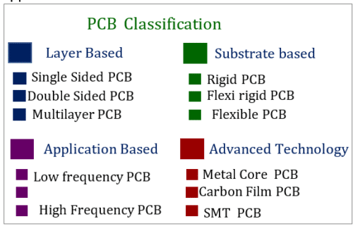
PCB Classification
Printed circuit boards can be classified according to fabrication processes and substrate materials such as:
- Layer based i.e. related to the number of layers
- Type of substrate material for fabrication i.e. organic or inorganic
- Physical structure or design i.e. rigid, flexible or semi
- Conductor pattern design based on application
Attributes like inorganic base, discrete wiring, additive, multi-wire and wire wrap were totally phased out as the technology advanced in all aspects.
Before getting into the details of PCB classifications, let us understand PCB terminology.
PCB Structure and Terminology
Transforming application design into a printed circuit board is a complex technological process. Designing the PCB while maintaining the standards with respect to Via hole, pad and anti–pads, lands and traces is another complex technological process.
PCB structure should match with the designer’s recommendations regarding fabrication of PCB size, maximum and minimum possible track width, minimum clearance between tracks etc.
Any manufacturing job order should be provided with guidelines about pad dimension requirements, Via requirements, fill requirements and maximum primitive dimensions so that these technical specifications are taken into consideration.
For example, if a track of 150 mil is required, a 100 mil track and a 55 mil track can be placed side-by-side with a 5 mil overlap to get a 150 mil track.
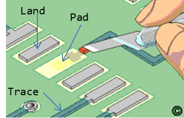
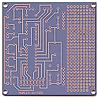
Traces and Spacing Between Them
A trace is a line of copper that makes an electrical connection between two or more points on a PCB. Traces carry current. The process of laying down traces on a PCB can be either plated or etched on the surface of the substrate to create the desired pattern. The method of etching is most common in the electronics industry.
The thickness of the copper on PCB is specified in ounces (oz)/square foot. In general, ½ oz and 1 oz copper are most commonly used. Thicker copper up to 6 oz is used for high current and reliability designs.
The design of trace width, trace thickness, spacing between traces, signal trace layouts, power and ground traces, and routing within the PCB layout are all based on design calculations and on-design rule standards. So why such calculations?
Track /trace width design is based on an individual current carrying capacity and maximum temperature resistance. The resistance to the current flow generates heat, which is dissipated by the trace depending on the surface area, airflow and solder mask thickness. Wider traces produce less heat that is dissipated easily.
Spacing between traces, in other words, electrical clearances is very important. It is recommended to have as much space as possible. The amount of spacing between tracks /traces and upper trace width is decided by the current flowing through it combined with the maximum temperature rise of the trace.
IPC has a set of standards about clearances and spacing charts based on environmental conditions (not voltage). Normally, signal traces maintain minimum width whereas power and ground trace widths are bigger and their spacing can be from 40µm – 60µm.
The part for edge spacing is important for the depanelizing process (minimum spacing of 125 mil is recommended).
Pads or Anti-Pads
Pads are small areas of copper used for connecting component pins. Anti-pad means that the pre-determined shapes are removed from the copper.
Generally, an anti-pad is used around a via to isolate it from a power plane where a connection is not needed.
Lands
Pads are needed to solder a component on the top or bottom layer of the printed circuit board, which are referred to as a land.
Pad size, shape and dimensions depend on:
1. Type of component package being used.
2. Manufacturing process used for assembling the board.
SMT pad-to-lead aspect ratio, THT hole-to-lead aspect ratio, THT annular ring, package sizes and pitch are defined by the IPC standards and design rules. Sometimes manufacturers define their choice. For example, the BGA pad size depends upon surface finish.
For HASL surface finish, BGA pad size will be 12 mil (1 mil = 0.001 inch) diameter and for other surface finishes, minimum 10 mil diameter will be maintained.
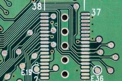
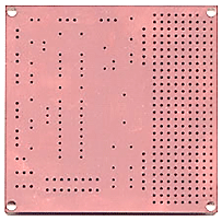
Via Holes
Via hole is a piece of metal that makes the connection between different layers of a PCB. It connects the traces from one side of the board to another by way of hole in the board. PTH (Plated Through Hole), Micro-Vias and Via in pad all come under the category of Vias.
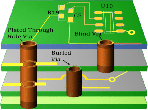
Vias carry signals or power between layers through PTH. The size of a Via depends on trace width. There are some Micro Vias used in between layers called Buried Vias, and between outer and inner layers called Blind Vias, that are used when high-density inner connections required.
Single-sided PCBs
Single-sided PCBs contain only one layer of conductive material and are best suited for low density designs. Parts are laid out on one side and the circuit on the other side.
The board is restricted in terms of circuit design because conducting happens on only one side, and no cross (conduction) is permitted. Each line must have its own path.
Single-sided PCB is the most basic and starting point for printed circuit technology. It is indeed the starting point of an invention as it plays a major role in the industry for low cost volume production of simple circuits.

Single-layer PCBs have a relatively wide field of applications ranging from power supplies, relays, sensors and LEDs to calculators, printers, coffee makers and electronic toys. However, single-sided PCBs feature some performance limitations as well.
Double-sided PCBs
It is the most common and widely used type of board. Double-layer PCBs have two conductive layers and traces that are placed on both sides of a substrate and so are the components. Due to increased complexity and density of components, many PCB’s need to use both sides.

The double sided plated-through-holes (PTH) PCB is the universal workhorse of the electronics industry. In plated-through-holes, copper connections go right through the connecting holes to the opposite side of the board.
These PTH connections either form simple electrical connections between both sides of the PCB (Via Holes) or produce electrical connectivity and mechanical support for leaded components.
This makes the double-sided PTH PCB a much more physically robust item, offering more flexibility for designers, low-cost and reduced board size (with increased circuit density).
Owing to these benefits, double-sided PCBs have covered a wide range of applications including power supplies, industrial control, control relays, converters, UPS system, LED lighting, hard drives, printers, mobile phone system, power monitoring, test equipment, amplifiers and traffic systems.
Multilayer PCBs
As the name implies, it is a PCB board with more than two, four, six, eight, thirty-five or even more layers. Many common features with double layered PCBs are:
- More than two layers with conductive traces, separated by insulating material between the layers.
- Layer between the conductive traces are connected through Vias with lamination as required.
The advantage of multilayer circuit boards is that with multilayer conductive wire and high density drilling, the volume becomes relatively small and the weight is relatively light. The high-density line reduces the space for components, which means more reliability. As there are more circuit layers, it is flexible for PCB design/layout.
Multi-layer printed circuit boards are the result of the development of high-speed, multi-function, high-capacity and small size electronic technology.
With the continuous development of electronic technology, especially for extensive application of large-scale and ultra-large-scale integrated circuits, the requirement of multilayer circuit PCBs with fine line width, small aperture through blind and buried Vias and high aperture ratio is important for developing high-density, high-precision and high-layer to meet the needs of the market.
Advantages of multilayer PCBs can be:
- Reduced board size and weight
- High level of density and flexibility
Capability to implement multiple functions that are better at dealing with interference allow designers to produce very dense and highly complex designs.
Quite often the extra layers in these designs are used as power planes, which supply the circuit with power that also reduce the electromagnetic interference levels emitted by designs.
Based on the merits mentioned above, multilayer PCBs are applied in products that require high technology and precision or those with higher space requirements like satellites, computers, GPS technology, servers, data storage, signal transmission, X-ray equipment, hand-held devices etc.
However, the disadvantages of having such boards are high cost and difficulty in testing.
Also Check: PCB Layout Design Guide
Types Of PCB
Rigid PCBs
It refers to those whose base material is a type of solid material that cannot be bent, for example, glass fibre. Typical PCBs can be categorised as rigid as they account for most boards.
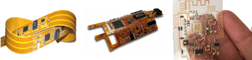
Rigid Flexi PCBs
It refers to boards using a combination of flexible and rigid boards. By removing the need for connectors and cables between the individual rigid parts, the board size and overall system weight can be reduced. This type of process is applicable while designing boards for cell phones, military, satellite, medical and automobile applications.
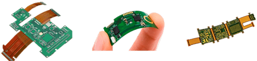
Flexible PCBs
These electronic circuits are formed by mounting electronic devices on flexible plastic substrates. These are ideal for high and flexible applications such as in automobile, disc drive, printers etc. However, repair work is impossible for flexible circuits.
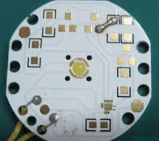
Aluminium backed PCBs
Typically used in high-power applications such as high-power LED products and switching power supplies, these boards provide ultimate solution for thermal heat dissipation and high-level mechanical tresses. The design keeps high-power components cool under heavy loads.
Basic Understanding of PCB Substrates
A substrate is also referred to as a dielectric material. It is an insulating material sandwiched between two conducting layers of PCB. When a PCB greater than two layers is constructed, a resin impregnated cloth material, commonly referred as PrePreg is used as a substrate.
Glass-reinforced substrate known as FR4, which is low-cost, flame resistant and water proof is the most used by PCB manufacturers.
For high frequency circuit boards i.e. high speed digital and radio frequency designs, a substrate comes in mostly three types:
- Fluorine – A high-cost dielectric substrate used for products with a frequency greater than equal to 5GHz.
- PPE resin
- Modified epoxy resin – Low priced and usually FR4 is used for products with frequency range of 1 -10GHz.
Polyimide is a substrate which is capable of functioning in high-temperature environments and is highly resistant to fire. This substrate is highly recommended for aerospace applications despite its water absorbent nature being a drawback, which is not relevant for this application.
PCB Fabrication
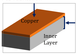
A single sided board is made from a rigid laminate, consisting of a woven glass epoxy base material clad with copper of varying thickness on one side.
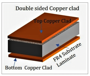
Double-sided boards are made from the same type of base material clad with copper of varying thickness on two sides. PrePreg or Preimpregnated Bonding Sheet acts as the “glue” that holds the cores together. There are many types of materials we can use. We use FR4 – a woven fibreglass cloth Preimpregnated with epoxy resin – known in the industry as B stage.
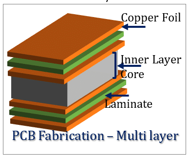
Multilayer boards are made from the same base material with copper foil on the top and bottom and one or more “inner layer” cores. The number of “layers” corresponds to the number of copper foil layers.
Multilayer fabrication begins with the selection of an inner layer core or thin laminate material of the proper thickness. Cores can vary from 0.038” to 0.005” thickness and the number of cores used will depend upon the board’s design.
Understanding the Fabrication Process
Copper Film – The copper foil used in circuit boards is typically in sheets of ½ oz and 1 oz per square foot in weight or 0.0007 and 0.00134 inches nominal thickness.
PCB Design Manufacturing Fabrication Process
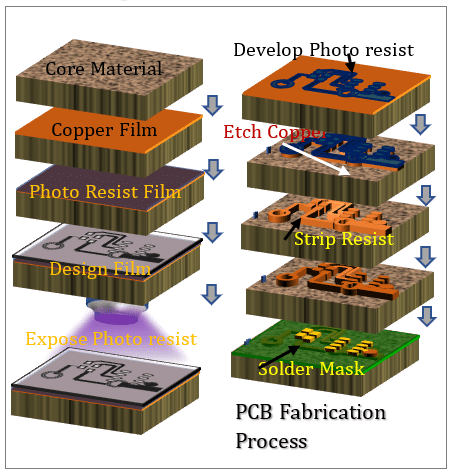
Step#1 – Film Generation
To generate your design files, we create an exact film representation of your design. We will create one film per layer.
Step#2 – Shear Raw Material
Industry standard 0.059″ thick, copper-clad are present on two sides. Panels will be sheared to accommodate many boards.
Step#3 – Drill Holes
By using NC machines and carbide drills, holes of various sizes can be created through a stack of panels (usually 2 to 3 high). The locations are determined by the board’s designer to fit specific components.

Step#4 – Electroless Copper
Once the smear is removed, a thin coating of copper is chemically deposited on all the exposed surfaces of the panel, including the hole walls. This creates a metallic base for electroplating copper into the holes and onto the surface. The thickness of the electroless deposit is between 45 to 60 millionths of an inch.
Step#5 – Apply Image
Apply photosensitive dry film (plate resist) to the panel. Use light source and film to expose the panel. Clear areas in the film allow light to pass through and harden the plate resist, creating an image of the circuit pattern.
Step#6 – Pattern Plate
Electrochemical process is used to build copper in the holes and on the trace area. Apply in to surface.

Note: All PCB express boards are plated through holes.
Step#7 – Strip & Etch
The developed dry film resist is now removed from the panel. The tin plating is not affected. Any holes that were covered with resist are now open and will be non-plated. This is the first step in the common phrase “strip-etch-strip” or ‘SES’ process.
Step#8 – Solder mask
A photo-sensitive epoxy-based ink is applied, completely coating the panel and later dried (but not cured). Using a method identical to photo formation, the panels are exposed to a light source through a film tool.
Then the panel is developed, exposing the copper pads and holes defined by the artwork. Solder mask is normally cured by baking in an oven.
However, some fabricators use infrared heat sources. Apply solder mask area to the entire board except for solder pads.
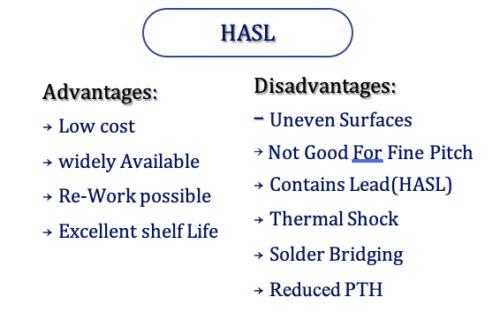
Step#9 – Solder Coat: (HASL Finish)
Apply solder to pads by immersing into a tank of solder. Hot air knives level the solder when removed from the tank.
Step#10 – Nomenclature
Apply white letter marking using screen printing process.
PCB Process Surface Finish Types
Surface finishes are designed to prevent oxidation of the remaining exposed copper, while solder mask covers majority of the circuit.
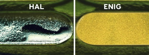
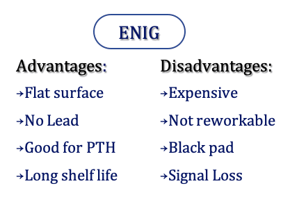
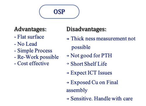
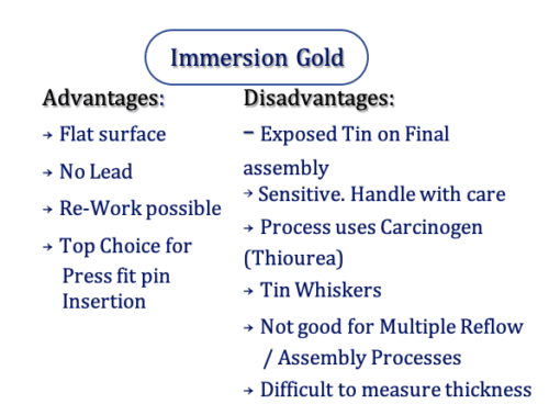
There are several types of surface finishes popularly known for Hot Air Surface Leveler (HASL), Electro Less Nickel Immersion Gold (ENIG), Immersion Silver, Organic Solderability Preservative (OSP), Electric Plating Gold Fingers, ENIG+OSP, ENIPIG etc.
Assembly of Flexible Circuits
The flux circuit fabrication is somewhat like a rigid PCB with a difference in using base material. Flex PCB assembly can only happen with the help of pallets. The following options can be chosen for Flex assembly manufacturing process.
Polyester soldering (<150°C) / Polyamide soldering (<300°C) is commonly opted for baking prior to assembly.
Flexible circuit construct with 0.05mm copper 18/18 µm as a base material and OSP, Immersion Nickel, Tin and Immersion Silver are options for solder finish.
To prevent warpage and support flexible circuit, use of Kapton sticky tape on the corner, pressure-sensitive low-tact tape magnets, clips and vacuum plates are the general practice for assembly process.
Assembly Pallet & Flex Circuit – Thermal relief areas on the base of pallet imposes Delta T during reflow. Also, consider drain holes under flex if the use of vapour phase leads to free reflows.
For flex circuit storage and baking, industry follows guidelines of IPC 1601 standards.
PCB RF Technology
Rapid advances in the use of RF/microwave low frequency bands have forced increased the density of RF/microwave devices to achieve escalating frequencies that are smaller, faster and cheaper.
Design of RF PCB is quite complex and needs to consider many factors in all aspects because RF PCBs are the backbone of RF technology. It drives satellite communication systems, broadband access and optical data networks.
In addition, an increasing number of automotive, industrial, military, homeland security, scientific and medical applications are using RF technology to perform detection, measurement and imaging functions.
Thermal management plays a very important role in the design of RF/microwave electronic devices. A large quantity of heat is generated when signals are processed in high-frequency applications, particularly in the amplification of high-frequency signals.
Reliable performance of an RF/microwave device depends on maintaining a constant value of the dielectric constant of the PCB’s dielectric layer.
Edge Plating
Encapsulating the edges of printed circuit boards with plating may be required to improve EMI shielding of higher frequency designs and to improve chassis ground in electronic systems
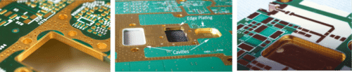
If the cavity is functioning as a RF/microwave resonant cavity, the frequency is determined by the size of the cavity and the PCB manufacturer must tightly control the X, Y and Z dimensions of the cavity. Cavity designs can be applied in multiple locations at different depths on a single printed circuit board and they can also be edge plated.
Also Check: Free Electronics Circuit and PCB Design + Simulation Software
Summary
PCB effects that are harmful to precision circuit performance include leakage resistances, IR voltage drops in trace foils, Vias and ground planes, the influence of stray capacitance and dielectric absorption (DA).
In addition, there is a tendency of PCBs to absorb atmospheric moisture. In general, the static or DC operation of the circuit especially at high frequencies.
Another very broad area of PCB design is the topic of grounding. Grounding is a problem area for all analogue and mixed signal designs. PCB designers never mix high frequency, high current circuits with low frequency, low current sensitive circuits and ensure to separate the grounds.
Even analogue and digital components are separated physically and electrically, especially their grounds.
Further, the outstanding characteristics of PCBs must have thermal stability, resistance to oxidation, acids, bases and other chemical agents like alkalis. It should have excellent dielectric properties, insoluble in water, soldering ability, reliability and reduce the risk of moisture intrusion.
About the Author
The author of this article is Mr. Adibhatla Krishna Rao, presently associated with NMTronics India Pvt ltd for the last 15years, having 26 years hands on experience in SMT manufacturing and service industry.
This technical content includes detailed descriptions about Electronic manufacturing processes and the manufacturing enterprise that can help aspirants, students and readers of these articles to know “a little about everything”.
References:
The relevant content of this report is based on author’s experience on PCB assembly manufacturing in different environments. To prepare this article, content material has been absorbed from various articles, white papers, published/released technical documents or uploaded in the Internet by famous scientists, SMT professionals and design engineers of OEMs.

Amazing article with very good content.
Thank You for your valuable feedback.
Very good and informative article sir. I am privileged to have seniors like you in NMTronics. Thanks again for enlighten us about PCB.