The sensor turns X-rays into signals on a chip, captures a wide light range, and enables low-cost imaging across medical, industrial, and environmental uses.
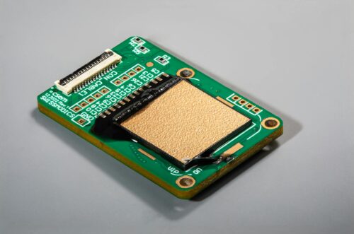
CSEM, in partnership with Dutch startup QDI Systems, has developed an image sensor that converts X-rays into electronic signals using quantum dots on a CMOS chip. This is the first time this method has been used. The sensor uses a spray-coated layer of quantum dots—semiconductor crystals that absorb specific wavelengths—placed directly on CMOS chips used in electronics. The sensor captures wavelengths from X-rays to visible light and short-wave infrared (SWIR). It provides spatial resolution, sensitivity from 400 to 1300 nm, and a fill factor close to 100%, maintaining pixel density and power use.

The sensor design removes the need for scintillators, hybrid bonding, and materials like InGaAs. The use of CMOS allows compatibility with semiconductor production lines, enabling large-scale fabrication at lower cost. This design combines spectral range and sensor function in one device, reducing the need for multiple systems.
The sensor can be used in healthcare for X-ray and mammography systems with lower radiation exposure. In industry, it allows testing of aircraft and machines without disassembly. In agriculture and recycling, it supports material sorting and crop analysis using SWIR imaging.
Some of the key features of the CMOS chip include:

- Turns X-rays into signals directly on the chip
- Uses tiny dots (quantum dots) sprayed on normal camera chips
- Works across X-rays, visible light, and short-wave infrared
- Almost all of each pixel is used for capturing images
The sensor was developed under the SWISSMODICS project for use in aircraft, with support from the EU’s Clean Sky 2 program and the Swiss State Secretariat for Education, Research and Innovation. It was first built to detect internal damage in aircraft. The same design is now being used in other areas such as inspection and monitoring. Nadim Maamari from CSEM said the sensor lowers cost and size limits, making imaging possible in areas that could not use it earlier.
For more information, click here.