


For the last four decades, planar or 2-D transistors, have been at the core of transistor design and architecture. In the image-2, we see a form of silicon that creates a stream (dotted yellow) through which electrons flow. The gate, which is made of metal over a material with high dielectric constant, controls the flow of electricity in that stream. It acts as an ordinary switch, turning flow on and off. That is, if an ordinary switch had the ability to turn itself on and off over 100 billion times a second! Technically, traditional 2-D planar transistors form a conducting channel in the silicon region under the gate electrode when in the “on” state. Talking about states, some key objectives in transistor design are to have as much current flowing as possible when in the “on state” for performance, to have as close to zero current flowing when it is in the “off” state to minimize power usage, and to switch very quickly between the two states again, for performance.
Now Coming to 3-D Transistors…

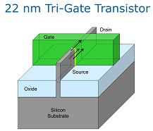
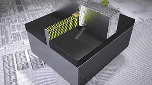
As transistors get ever smaller, one way to achieve this is to get tighter control, by having the gate wrap around the channel as much as possible. The animated version of the transistor can be seen in image-3. With Intel’s 3D transistor’s architecture, the flat two dimensional stream has been replaced with one or more three-dimensional fins as shown in the image-4.
The control is on all the three sides of each fin, rather than just one, as in the the Planar 2-D transistor. In simpler terms, the transistor channel is raised into the 3rd dimension. Current flow is controlled on three sides of the channel (top,left and right). This is called a Tri-Gate transistor and its real advantage over Planar is the ability to operate at lower voltage with lower leakage, providing an unprecedented combination of improved performance and energy efficiency. This breakthrough invention allows Intel to create transistors that are smaller, faster and use less power than ever before, enabling a new generation of computing technology in every category, from the fastest super computers to the smallest hand-held devices. Tri-Gate transistors can have multiple fins (as shown in image 5) connected together to increase total drive strength for higher performance.

The Real Deal With 3D
The 3-D geometry and structure of the Tri-Gate transistor provides a host of important improvements over the planar transistor structure, all related to the ‘wrap-around’ effect of the MOSFET ‘gate’ around the source-to-drain ‘channel.’ These advantages manifest in improved performance, reduced active and leakage power, transistor design density, and a reduction in transistor susceptibility to charged particle single event upsets (SEU).
The power advantage results from the improved control of the channel by the gate’s electric field on three sides of the fin. As explained by Intel Corporation at their Intel Developer Forums (2011, 2012), this power advantage is created by an effectively steeper transistor voltage curve for Tri-Gate transistors. Transistor designers can take advantage of this steeper curve with either a significant reduction in leakage current for the same performance of a planar transistor, or substantially higher performance (transistor operation speed), or a combination of both.
The Real Advantage of Tri-Gate Transistors
·More than 50% power reduction at constant performance.
·37% performance increase at low voltage.
·Improved performance and efficiency.
“For years we have seen limits to how small transistors can get,” said Gordon E. Moore. “This change in the basic structure is a truly revolutionary approach, and one that should allow Moore’s Law, and the historic pace of innovation, to continue.” – Gordon E. Moore
“The performance gains and power savings of Intel’s unique 3-D Tri-Gate transistors are like nothing we’ve seen before. This milestone is going further than simply keeping up with Moore’s Law. The low-voltage and low-power benefits far exceed what we typically see from one process generation to the next. It will give product designers the flexibility to make current devices smarter and wholly new ones possible. We believe this breakthrough will extend Intel’s lead even further over the rest of the semiconductor industry.” – Mark Bohr, Intel Senior Fellow
[stextbox id=”info” caption=”FUN FACTS: EXACTLY HOW SMALL (AND COOL) IS 22 NANOMETERS?”]
The original transistor built by Bell Labs in 1947 was large enough that it was pieced together by hand. By contrast, more than 100 million 22nm tri-gate transistors could fit onto the head of a pin*.