


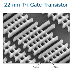
More than 6 million 22nm tri-gate transistors could fit in the period# at the end of this sentence.
A 22nm tri-gate transistor’s gates that are so small, you could fit more than 4000 of them across the width of a human hair^.

If a typical house shrunk as transistors have, you would not be able to see a house without a microscope. To see a 22nm feature with the naked eye, you would have to enlarge a chip to be larger than a house. (4)
Compared to Intel’s first microprocessor, the 4004, introduced in 1971, a 22nm CPU runs over 4000 times as fast and each transistor uses about 5000 times less energy. The price per transistor has dropped by a factor of about 50,000.
A 22nm transistor can switch on and off well over 100 billion times in one second. It would take you around 2000 years to flick a light switch on and off that many times**.
It’s one thing to design a tri-gate transistor but quite another to get it into high volume manufacturing. Intel’s factories produce over 5 billion transistors every second. That’s 150,000,000,000,000,000 transistors per year, the equivalent of over 20 million transistors for every man, woman and child on earth.
*A pin head is about 1.5 mm in diameter.
#A period is estimated to be 1/10 square millimeter in area.
^A human hair is about 90 microns in diameter.
(4)The smallest feature visible to the naked eye is 40 microns.
**Assumes a person can flick a light switch on and off 150 times per minute.
Table Courtesy – Intel’s Press Material on 22 nm 3-D transistor technology
[/stextbox]
Tri-Gate Devices Now in Production
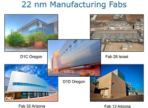
The advanced state of semiconductor manufacturing at very small geometries (40 nm, 28 nm, 22 nm or 20 nm and beyond) requires research and development expenditures that now limit this technology to a handful of companies with capital expenditure capabilities in the billions of dollars. As a result, only a handful of manufacturers are able to capitalize on the known advantages of 3-D transistor technology. Intel Corporation is the only company to have made this design and manufacturing transition in 22 nm technology, and can provide data on the overall maturity and manufacturability of Tri-Gate transistors on a mass production scale. This data, as of the first quarter of 2013, includes 100 million units of Tri-Gate transistorbased products.
Several known issues and characteristics of the 3-D gate structure have been acknowledged and addressed to achieve manufacturing and design maturity with the technology. These include the modeling of new parasitic capacitance values not modeled in traditional planar designs, layout dependent effects, and the use of double-patterning techniques using current lithographic equipment to form closely spaced fins. A great deal of publicity and user education is underway in 2013 by companies like Cadence and Synopsys revolving around the impact of Tri-Gate rules and flexibility in the design of future semiconductor products.
Impact on FPGA and Other Semiconductor Device Performance
Let’s see how this three dimensional technology will provide a significant boost in the capabilities of high-performance programmable logic.
The primary advantage of Tri-Gate technology to FPGA-based electronic product designer is the continuation of Moore’s Law in the steady march of improvements in transistor density, performance, power, and cost-per-transistor. This sustains an industry of consumer electronics, computing platform development, software complexity advances, memory and storage growth, mobile device creativity and development, and business automation and productivity.In addition, control over the static and active power dissipation of semiconductors improves tremendously with this technology. For users of FPGAs, this makes programmable logic that advances to 14 nm technology and beyond both power competitive with ASIC and ASSP design solutions on available competing design nodes, with even more significant advantages in programmability, performance, flexibility, Open Computing Language (OpenCL™) software design entry, and integration of DSP, transceiver, hardened processor, and configurable I/Os.
