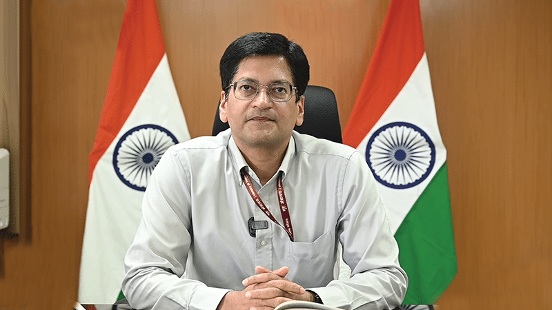
Launched in 2021 and operationalised in 2022, the India Semiconductor Mission (ISM) is driving India’s ambition to build a self-reliant semiconductor ecosystem spanning manufacturing, design, talent, and supply chains. In this exclusive interview, Dr Satya Gupta, President of the VLSI Society of India (VSI), speaks with Shri Amitesh Kumar Sinha, Additional Secretary, MeitY, and CEO of ISM, about the mission’s progress, challenges, and roadmap for India’s semiconductor future.
Q. You have been associated with the ISM since its inception. Looking back over the past four-and-a-half years, how would you assess its progress, achievements, and key challenges?
A. The Union Cabinet approved the India Semiconductor Policy and the ISM on 15th December 2021, marking India’s first comprehensive semiconductor policy backed by a long-term vision and strong commitment from Prime Minister Shri Narendra Modi and the Union Minister of Electronics and Information Technology, Shri Ashwini Vaishnaw.

Our biggest challenge at the outset was the absence of a semiconductor ecosystem. Without one, attracting global manufacturers is extremely difficult. The first proposals we received were not sufficiently convincing, and because semiconductor manufacturing is highly complex, particularly for a first-time entrant like India, we approved only those projects with a high probability of success.
To ensure this, we established rigorous evaluation criteria and constituted committees of global techno-commercial experts. Every project had to satisfy three non-negotiable requirements:
• Strong financing. Applicants needed deep financial strength backed by profitable or cash-rich parent companies capable of withstanding the cyclical nature of the semiconductor industry. Many early applicants were attracted primarily by government incentives, so identifying genuinely committed partners took time.
• Credible technology transfer. We required complete production-ready technology transfer rather than simple licensing agreements. This included equipment specifications, workforce training, utility planning, installation support, prototype wafer runs, and qualification processes.
• Customer off-take. Technology partners had to commit production and bring established customers, giving global buyers confidence in India’s new manufacturing facilities.
The first company to meet all three criteria was Micron Technology. As an integrated device manufacturer (IDM), it already possessed financing, proprietary technology, and captive demand. Its entry was a turning point, signalling India’s seriousness to the global semiconductor industry.
That breakthrough was followed by strong proposals from Indian companies, including Tata Electronics for wafer fabrication and packaging, and packaging proposals from CG Power and Industrial Solutions and Kaynes Technology.
Our advisory committee, comprising leading members of the Indian diaspora and global semiconductor experts, also helped refine the policy. They recommended simplifying incentives and making them uniform across silicon, display, and compound semiconductor fabs, as well as assembly, testing, marking, and packaging (ATMP) facilities. They also advised that packaging would naturally precede fabrication, helping establish the broader ecosystem. Today, we have approved 12 semiconductor projects under this framework.
Alongside manufacturing, we recognised that semiconductor design is one of India’s greatest strengths. Under the Design-Linked Incentive (DLI) scheme, 24 companies have received financial support, while more than 100 companies have been given access to world-class electronic design automation (EDA) tools following rigorous technical and commercial evaluation. Significantly, 15 of these startups have already secured institutional venture capital funding, with further investment continuing to flow into the ecosystem.
The Tata Electronics semiconductor fab at Dholera, Gujarat, represents another major milestone. Building India’s first wafer fab has been a nationwide learning exercise involving Tata Electronics, Powerchip Semiconductor Manufacturing Corporation (PSMC), the ISM, central and state governments, and construction partners such as Larsen & Toubro (L&T) and Tata Projects. Together, we have gained valuable experience in specialised infrastructure, uninterrupted power and water supply, logistics, customs, international talent, equipment movement, and regulatory requirements, while continuously refining policies to address emerging challenges.
We expect commercial production from the Tata fab to begin by 2028. Furthermore, market demand is already encouraging. Tata has secured strong customer interest across multiple technology nodes, exceeding the capacity of its initial facility. Our packaging programme has progressed even faster. Micron Technology has already started commercial production, Kaynes Technology has commenced manufacturing, and two more ATMP projects are expected to begin production later in 2026. Overall, this has been an excellent start to India’s semiconductor journey.
So, all these developments in the last four-and-a-half years have given us a good base, and it has created confidence in Indian industry, as well as outside India, and as a result of that, now we are seeing a lot of traction from foreign companies from Japan, South Korea, Singapore, Malaysia, Europe, and the US. They are looking at the Indian market strategically and they clearly understand that there is a scope of development here. The semiconductor industry is going to happen here. This kind of confidence building is the greatest satisfaction, and we believe that going forward, we will attract more and more companies.
In a nutshell, the incentive amount announced by the government of India is now fully committed, and we have 12 manufacturing and 24 design projects with us.
Q. When ISM 1.0 was formulated, the 28nm node was widely considered the optimal starting point for India. When do you expect India to have operational 28nm production for domestic chip designers?
A. The more mature nodes above 28nm should enter commercial production by 2028, while 28nm production is expected by 2029.
Q. So, India can realistically expect indigenous commercial production at the 28nm node by around 2029?