
SEPTEMBER 2011: Big things come in small packages. This statement holds 100 per cent true for light-emitting diodes (LEDs), which are now celebrated for many salient features including small form factor, long life and low power consumption.
That said, you might be surprised to learn that the first LEDs were far from being useful. They could only operate at bizarre temperatures of -77ºC and below, would burn out in only a few hours, guzzle power like demons, and produce very little light in the bargain. As we can see, all of these cited weaknesses have over time transformed into strengths—mainly due to process and material improvements. In short, the technological and business developments in the LED industry have been, and continue to be, evolutionary and revolutionary at the same time.

In the past few years, improvements in efficacy, packaging and price of LEDs have resulted in a greater realisation of its benefits, more applications and a larger market. “The range of applications for LEDs continues to grow significantly. One of the fastest growing and most promising uses is in illumination applications. LEDs are penetrating this market rapidly due to the combination of excellent colour saturation and energy savings that satisfy today’s demand for reduced energy ‘green’ products, and long life,” explains Hari Kiran Chereddi, managing director, Sujana Energy.
“LEDs are one of the most energy efficient and green lighting solutions available today, and this has been the primary reason for their rapid popularity across the world, amid rising awareness about the environment. These are one of the most sustainable and long-lasting lighting sources and facilitate reduction in carbon dioxide emissions, in addition to helping save energy and maintenance costs,” adds Indranil Goswami, head-lighting application services, Philips Lighting India.
In this article, we take a quick look at the recent improvements in LED technology and its exciting applications, as also the challenges that continue to daunt the industry. However, before we foray into the details, it might be wise to begin with Chereddi’s simple summary of recent developments: “As LED materials technology became more advanced, the light output has increased, and LEDs have become bright enough to be used for illumination. But, with higher power, it became increasingly necessary to get rid of the heat, so the packages have become more complex and adapted for heat dissipation. The efficacy of white LEDs has risen from about 15 lumens per watt (lm/W) to over 100 lm/W. In the past two years, there has been a significant fall in the cost of LEDs; the reasons behind the price fall are mass manufacturing and improved technology.”
[stextbox id=”info” caption=”Understanding LEDs”]

In order to understand the improvements in LED technology, it is very important to know the basics of how an LED works and how it is made.
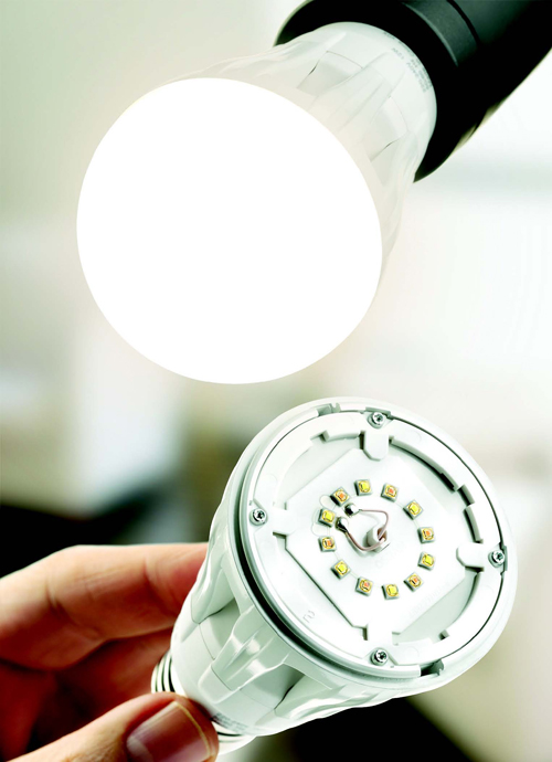
Concept. Diodes are electrical valves made of very thin layers of semiconductor material. One layer will have an excess of electrons, while the next will have a deficit of electrons. This difference causes electrons to move from one layer to another, thereby generating light. More the number of electrons crossing from one layer to another, brighter the light generated.
Construction. A semiconductor is a crystalline material. It conducts electricity only when there is a high density of impurities in it. The semiconductor wafer is a single uniform crystal—for the purpose of LEDs, the semiconductors are usually made from gallium arsenide (GaAs), gallium phosphide (GaP) or gallium arsenide phosphide (GaAsP). Once the slice or wafer of semiconductor is ready, various impurities like zinc, nitrogen, silicon, germanium or tellurium are suspended in it through a process called doping; there are various techniques for this. The impurities create a layer with excess or deficit electrons. Once these layers are ready, wires are stuck to the semiconductor to introduce electricity. This completes the LED device. Depending on the semiconductor materials (called substrates) and the impurities used, the LED produces different colours of light.
Challenges. The key to successfully designing and manufacturing LEDs is to understand that it is both an electronic and optic device, affected by electrical, electronic and optic principles. Properties such as colour, brightness and efficiency are affected by the size of the diode, the semiconductor materials used to make it, the thickness of the diode layers, the type and amount of impurities used to dope the semiconductor, etc. The goal of an LED designer is to optimise these parameters.
[/stextbox]
All key parameters seem to be on the rise
Most of the key parameters used to evaluate LEDs such as light output (flux), efficacy (lm/W), colour quality and stability have improved greatly in the recent past, thanks mainly to material sciences and semiconductor fabrication technologies. “LED technology has been evolving rapidly since the last one or two years. The diode technology has improved significantly and as a result high-power LEDs with higher lumen output are making it possible to replace other lamps with LED lamps. This has resulted in wider application of LEDs. The past few years have also seen a remarkable improvement in the efficacy of LED chips, packages and lamps, measured in terms of the number of lumens emitted per watt of electrical power consumed,” says Goswami.