


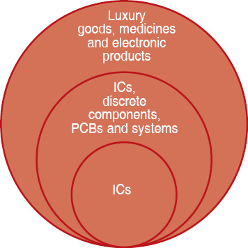
Counterfeiting ranges from exact copies of whole products to replicas of electronic components. With the increasing need for components, counterfeiters are becoming sophisticated and are using advanced techniques to counterfeit. Fig. 1 shows what all are getting affected by counterfeiting.

With increased outsourcing of both ICs and product manufacturing, original equipment manufacturers and original component manufacturers have lesser control over the manufacturing process, which is leading to the proliferation of counterfeit components/products in the market.
Types of counterfeits
Counterfeits are classified by the way these are fabricated and fall into the following categories:
Recycled. Devices that are pulled out of discarded printed circuit boards (PCBs), which are sent for recycling, are modified in such a way that these look like new ICs, which are then sent out for sale.
Re-marked. Each semiconductor is marked in a unique way in order to identify its function, data it contains, place of manufacture, part identification number, manufacturing batch number, date code and electrostatic discharge sensitivity code. Normally, MIL- and space-grade products carry a higher price tag. Counterfeiters mark the regular commercial parts as MIL grade or space grade, and sometimes industrial grade, and sell these at a higher price.
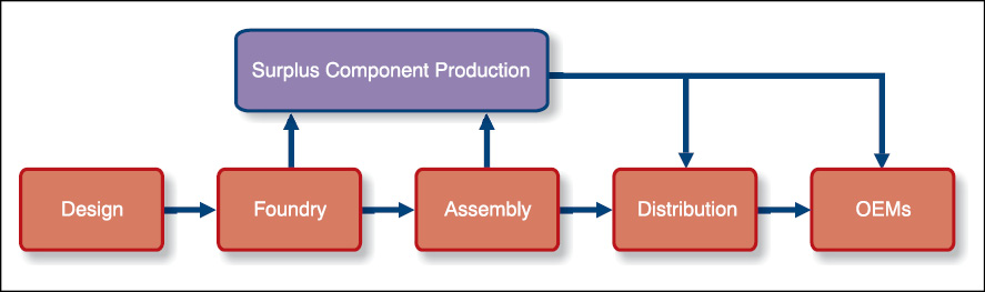
Over-produced. With increased proliferation of fabless semiconductor vendors (IC manufacturers who do not own a foundry and use a third-party foundry for manufacturing the ICs, and are very similar to electronics manufacturing service (EMS) vendors), foundries that manufacture ICs produce more than the required quantity and sell these in the market. This typically happens with unreliable foundries. Fig. 2 shows the leakage points where devices can leak out of the system and get into the market.
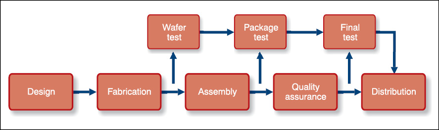
Rejected or defective. Counterfeits that fall into this category are devices that are rejected in one of the test stages in the manufacture of an IC, as shown in Fig. 3.
A typical semiconductor has three stages of testing: first, at wafer level, second, when the device is packaged and third, during final testing. Any device that fails any one of the three test stages is rejected and sent for destruction. The failure could be from downright dead devices to devices that fall outside test specifications. Counterfeiters pick up these rejected items and sell these back to the market as good parts.
Cloned. With increased use of third-party-developed IP cores (codes/circuits that are tested and available in a reusable format), cloning has become quite easy. Typically, cores are licensed for a fee and chip designers integrate these into their designs. Counterfeit manufacturers use the IP core in their devices without paying the licence fee to the developer and get the ICs manufactured.
In addition, when complexity of ICs is low, some counterfeiters just reverse-engineer the whole IC and clone it or copy it. Detection of clones is a challenge as in most cases these function like the originals.
Forged documentation. Another type of counterfeits tamper the documentation that is sent along with the ICs when shipped from factories. By forging documentation, devices can be up-marked (represented as a higher specification part) and sold at a higher price. A good example is to mark a commercial-grade part as industrial-grade.
Defects found in counterfeits
There are two types of defects: internal or invisible defects and external or visible defects. Internal defects are generally called package defects, whereas external defects are further classified into two categories:
Procedural defects. These mainly relate to the packaging and shipping of components and their markings
Mechanical defects. These are due to structural deficiencies and can be further classified as:
Leads/balls/columns. Damages found in leads of different IC packages
Package dimensions and type. Deviations in the IC package from standard packages as defined by JEDEC standards
External defects occur due to reuse of devices, processes used in getting the devices ready for reuse, especially while pulling out of PCBs.
Internal defects are not visible and are invariably associated with the internals of ICs, which could have happened either in the foundry or at the package-assembly stage.
When ICs are manufactured, the die is attached to wire frames. Depending on the design parameters, designers use either a single wire or two wires for bonding the die to the leads. Most counterfeit ICs have either one or both these burnt due to usage.
Another internal fault is the damaged die inside ICs. This happens either due to the process or de-lamination. At this stage, we need to remember that a counterfeit may not be functional.
Detecting counterfeits
Detection of counterfeits is a time-consuming and intensive process. Proper supply chain checks need to be in place for detecting counterfeits early on in the process; detecting these just as these enter the inventory is the best way to avoid problems.
There are several tests that could be performed to detect counterfeits.
First is a physical test, using incoming inspection or an automated image-recognition system for inspecting the information printed on the package.
Second is a destructive test in which samples are physically destroyed to find counterfeits.
The third uses sophisticated tests like X-ray spectrometry or material analysis for accurate detection.
Another type of detection involves electrical parameter testing. These tests either check the electrical parameters or subject the counterfeits to burn-ins to check durability of parts. At times, all these tests are carried out to identify counterfeits.
How to avoid counterfeiting
Avoiding counterfeits is a tricky and expensive process. However, compared to the cost of the bad impact of counterfeits on products, a little price paid for avoiding is better in the long run. Avoiding counterfeit parts needs proactive and real-time actions.
First step is to control the supply chain so that the purchase process is robust, and all data of purchased components is logged and kept for future reference. This data is typically captured and kept when avionics and medical devices are manufactured. For other products, it is basically the manufacturing process that addresses this aspect.
Proactive avoidance mechanism in the design and manufacturing of ICs makes counterfeiting as difficult as possible. Proactive avoidance techniques include avoiding die and IC recycling (includes two methods of combating counterfeiting, namely, anti-fuse based avoidance and ring oscillator based avoidance), watermarking of ICs, physical unclonable functions and secure split tests.
Let us now see how counterfeiting is being tackled at design level.

Combating die and IC recycling (CDIR). Bulk counterfeiting happens at foundry and assembly locations, and there are two basic technologies that are used. First is anti-fuse/fuse based technology, which is similar to the technology used in programmable logic devices.
Essentially, when an IC with anti-fuse protection powers up, for a brief moment, the programmable logic is in read mode and the central processing unit (CPU) is able to read and verify the authenticity of the device by comparing it with the data supplied by the vendor. Since it requires programming of each device, this technique is used for high-value ICs like CPUs, precision analogue-to-digital converters and graphics processing units.
For low-cost devices, the solution is a little more ingenious. Typically, a semiconductor fuse is introduced in the IC, which gets blown during testing. So if a counterfeit IC has been used, which could either be a recycled IC or counterfeit die, the blown fuse will indicate that the device is a counterfeit. Fig. 4 shows how this is implemented.
One risk to the above approach is that counterfeiters can easily crack current technologies, so more complex counterfeit-avoidance mechanisms should be used.
One method that is quite popular and difficult to crack is the ring oscillator based CDIR. In this design, as part of the IC, two ring oscillators are introduced; a ring oscillator is a circuit in which several inverters are connected in series and the output is connected to the input so that the circuit oscillates. One of the oscillators is such that it ages faster (so the frequency changes) than the other, so that as the ICs work, the frequency of oscillation will not be the same as it was when it was produced (which can be measured with the other oscillator, which is part of the IC).
IP copying. Another popular counterfeiting is the copying or unlicensed usage of IP cores. With an increase in pressure on time-to-market, most semiconductor designers use off-the-shelf IP cores, which are tested and proven, and can be included in the IC design directly as a library.
As a business practice, companies sell the core typically under licence to the user under trust. However, if the licensee uses it without the IP owner’s licence, it becomes difficult for IP companies to track and prevent copying.
With increased sophistication in counterfeiting, protection of IP with advanced techniques has become a necessity. The most popular method is encryption, in which only when the authorised key is used, the code is enabled. This works when the IP is in the form of hardware description language (HDL) codes. In case of a hard IP, where it is in the form of a proven module, other techniques need to be used.
A popular technique for avoiding counterfeiting is watermarking. Normally, watermarking impacts the item that is being watermarked, but in the case of IPs this is not desirable. So most watermarking is done either by using constraints (known way of doing things) or additive to hardware IP. This way watermarks are distinctly visible.
Another popular counterfeit-avoidance technique uniquely identifies the IC so that it can be traced back to the original chip manufacturer. This technique is known as physically unclonable function (PUF). It is close to the biometrics collected for human beings and is called silicon fingerprints.
PUF implementation depends on the fact that process variation happens during fabrication of ICs and each chip has a distinct identity. Silicon PUF is a circuitry that extracts random characteristics out of an IC and, using those, generates a unique signature. By using a challenge-response protocol, which is similar to challenge handshake authentication protocol and password authentication protocol used in networking, the signature can be extracted and compared with the response already collected during manufacturing.
The challenge and response bits are known as challenge-response pairs. Response bits are known as PUF signatures. Silicon PUFs have turned out to be a good antidote for counterfeiting.
PUF signatures are either delays caused by process variations or by using aging-resistant ring oscillators, which have a frequency difference due to process variation.
While this sounds easy, there are certain challenges in implementing this technology such as:
1. Getting a stable response over a widely varying environment
2. Implementing parts that are already in use
3. Taking care of implementation costs
4. Securely storing and maintaining the servers to store challenge-response pairs
Another technique that supplements this technique is encrypted QR codes on the packaging of the IC, which allow identification when decrypted with proper keys.
Finally, a popular technique that ensures that counterfeits do not leak from foundry and assembly locations is known as the secure split test, also known as connecticut secure split test (CSST).
In Fig. 3, we can see leakages when ICs get rejected after testing. To plug this, CSST is implemented, in which a structure is added to the IC and the test response is uniquely perturbed. This process is devised by the IP owner, who alone can examine the test result through a proprietary communication and decide whether the device is genuine or counterfeited. If the IC is genuine, the IP owner sends the key to open the lock to the foundry and only then the IC is usable. Using this technique, the problem of over production can be addressed by keeping track of the number of keys that are released.
This technique also prevents IP cloning as the IP can be opened only with the right key issued by the IP owner.