


From chip design to testing, India moves to localise silicon photonics, building tools that could reshape both classical and quantum hardware development.
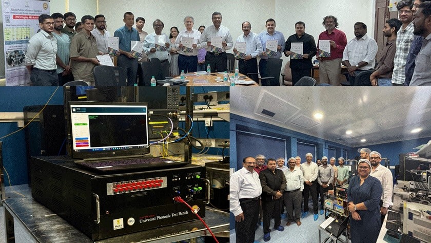
The Ministry of Electronics and Information Technology (MEITY) has launched two indigenously developed silicon photonics solutions, marking a step toward domestic capability in photonic chip design and validation. Developed at IIT Madras under the CoE CPPICS initiative, the release includes a Silicon Photonics Process Design Kit and a Universal Programmable Photonic Integrated Circuit Test Engine.

The Process Design Kit provides a library of more than 50 verified components, enabling designers to build photonic integrated circuits using a standardized, fabrication ready framework. This reduces dependency on external toolchains and supports local development across startups, research institutions, and defence applications. By offering a structured design environment, the PDK lowers entry barriers for photonic IC development, an area traditionally limited by access to specialised infrastructure.
Complementing the design layer, the programmable photonic test engine functions as an automated characterisation platform. It allows evaluation of photonic and optoelectronic modules across different operating conditions, supporting validation, benchmarking, and system level testing. Together, the two systems address a critical gap between design and deployment in photonics workflows.
From a technology perspective, the initiative aligns with CMOS compatible silicon photonics, enabling integration with existing semiconductor manufacturing processes. The centre follows a Product Research, Development and Manufacturing model, with fabrication support from SilTerra Malaysia and packaging handled by izmo Microsystems.
The development also connects to broader national ambitions under the India Semiconductor Mission, where future phases may include multiproject wafer runs, packaging ecosystems, and potential domestic fabrication capabilities.
“Starting in Q3 of this financial year, our center will enable Silicon Photonics MPW fabrication runs while offering comprehensive testing, packaging, and module characterization,” says, Chief Investigator Prof. Bijoy Krishna Das.
The launch signals a shift toward building an end to end silicon photonics ecosystem within the nation, spanning design tools, validation platforms, and manufacturing pathways.