


A Metal Oxide Semiconductor Field-effect Transistor (MOSFET, MOS-FET, or MOS FET) is a field-effect transistor (FET with an insulated gate) where the voltage determines the conductivity of the device.
It is used for switching or amplifying signals. The ability to change conductivity with the amount of applied voltage can be used for amplifying or switching electronic signals.
MOSFETs are now even more common than BJTs (bipolar junction transistors) in digital and analog circuits.
The silicon dioxide forms the Gate of the MOSFET. It is used to provide isolation by preventing the direct flow of charges on the gate to the conducting channel.
A MOSFET is by far the most common transistor in digital circuits, as hundreds of thousands or millions of them may be included in a memory chip or microprocessor.
Since they can be made with either p-type or n-type semiconductors, complementary pairs of MOS transistors can be used to make switching circuits with very low power consumption, in the form of CMOS logic.
Why Choose MOSFET Over BJT?
MOSFETs are particularly useful in amplifiers due to their input impedance being nearly infinite which allows the amplifier to capture almost all the incoming signal. The main advantage is that it requires almost no input current to control the load current and that’s why we choose MOSFET over BJT.
Structure:
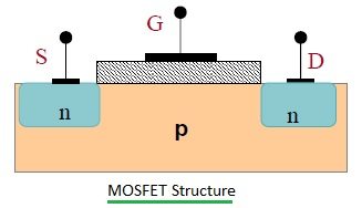
It is a four-terminal device with Source (S), Drain (D), Gate (G), and body (B) terminals. The body (B) is frequently connected to the source terminal, reducing the terminals to three. It works by varying the width of a channel along which charge carriers flow (electrons or holes).
The charge carriers enter the channel at the source and exit via the drain. The width of the channel is controlled by the voltage on an electrode called Gate which is located between the source and the drain. It is insulated from the channel near an extremely thin layer of metal oxide.
A metal-insulator-semiconductor field-effect transistor or MISFET is a term almost synonymous with MOSFET. Another synonym is IGFET for the insulated-gate field-effect transistor.
Different Types of MOSFET
MOSFET works in two modes-
1. Depletion Mode: The transistor requires the Gate-Source voltage (VGS) to switch the device “OFF”. The depletion-mode MOSFET is equivalent to a “Normally Closed” switch.
2. Enhancement Mode: The transistor requires a Gate-Source voltage (VGS) to switch the device “ON”. The enhancement mode MOSFET is equivalent to a “Normally Open” switch.
Now with respect to the working principle, MOSFET is classified as follows:
- P-Channel Depletion MOSFET
- P-Channel Enhancement MOSFET
- N-Channel Depletion MOSFET
- N-Channel Enhancement MOSFET
P-Channel MOSFET
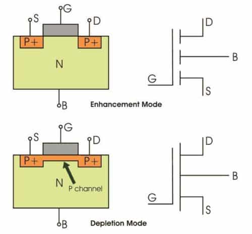
The drain and source are heavily doped p+ region and the substrate is in n-type. The current flows due to the flow of positively charged holes, and that’s why known as p-channel MOSFET.
When we apply negative gate voltage, the electrons present beneath the oxide layer experience repulsive force and are pushed downward into the substrate, the depletion region is populated by the bound positive charges which are associated with the donor atoms.
The negative gate voltage also attracts holes from the P+ source and drain region into the channel region.
N-Channel MOSFET
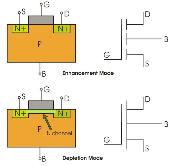
The drain and source are heavily doped N+ region and the substrate is p-type. The current flows due to the flow of negatively charged electrons and that’s why known as n-channel MOSFET.
When we apply the positive gate voltage, the holes present beneath the oxide layer experience repulsive force, and the holes are pushed downwards into the bound negative charges which are associated with the acceptor atoms.
The positive gate voltage also attracts electrons from the N+ source and drain region into the channel thus an electron-rich channel is formed.
MOSFET Working Operation
The working principle of a MOSFET depends upon the MOS capacitor. The MOS capacitor is the main part of MOS-FET. The semiconductor surface at the below oxide layer is located between the source and drain terminals. It can be inverted from p-type to n-type by applying positive or negative gate voltages.
When we apply positive gate voltage, the holes present under the oxide layer experience a repulsive force, and holes are pushed downward with the substrate.
The depletion region is populated by the bound negative charges that are associated with the acceptor atoms. The electrons reach, and the channel is formed. The positive voltage also attracts electrons from the n+ source and drain regions into the channel.
Now, if a voltage is applied between the drain and source, the current flows freely between the source and drain and the gate voltage controls the electrons in the channel. If we apply negative voltage, a hole channel will be formed under the oxide layer.
Applications
- Amplifiers
- Regulation for DC Motors
- Constructions of Chopper Amplifiers
- Switching and Amplifying Signals
People Also Ask
How does a MOSFET work?
A voltage applied to the gate controls the current flowing between drain and source by forming or depleting a conductive channel.
What is gate threshold voltage (Vth)?
The minimum gate-to-source voltage required to start forming a conductive channel.
What is Rds(on)?
The on-state resistance between drain and source when the MOSFET is ON. Lower Rds(on) = lower conduction losses.
What is a logic-level MOSFET?
A MOSFET designed to fully turn ON at low gate voltages (2.5–5V), making it compatible with microcontrollers.
What is body diode in MOSFET?
An inherent diode between drain and source that conducts during reverse polarity. It’s important in motor control, buck converters, and H-bridge designs.
What happens if a MOSFET’s gate is left floating?
It may turn ON/OFF unpredictably due to noise. Always pull gate HIGH or LOW using a resistor.
Why do MOSFETs require a flyback diode in inductive loads?
To protect against high voltage spikes generated by coils, motors, and relays.
What is MOSFET safe operating area (SOA)?
It defines safe limits for voltage, current, and power dissipation to prevent thermal or avalanche damage.
What is MOSFET gate charge (Qg)?
The total charge needed to fully switch the MOSFET ON. Lower Qg = faster switching.
What is thermal runaway in MOSFETs?
When heat increases Rds(on), causing more heat—leading to device failure.
What is a MOSFET driver and why is it needed?
A gate driver boosts the gate voltage and provides fast current pulses, ensuring optimal switching at high frequencies.
Which force acts on holes under the oxide when positive gate voltage is applied (MOS capacitor)?
A negative electric field (from the positive gate) attracts electrons to the semiconductor surface and repels holes; the holes experience an electrostatic force pushing them away from the oxide interface. This field causes band bending and, for sufficiently positive gate voltage (NMOS), creates an inversion layer (electron channel) by attracting electrons.
Does a MOSFET’s gate have a direct physical (DC) connection to the semiconductor?
No. The gate is separated from the semiconductor by an insulating gate oxide (ideally SiO₂ or a high-k dielectric). That means no DC current should flow into the gate (very high input impedance). Gate control is capacitive—the gate voltage creates an electric field that modulates channel conductivity.
Is the MOSFET gate oxide aluminum oxide or silicon dioxide?
Historically the gate insulator is silicon dioxide (SiO₂). Modern processes may use high-k dielectrics (e.g., HfO₂) to reduce leakage while increasing capacitance. Aluminum oxide is not the standard gate dielectric in mainstream MOSFET processes.
What determines the conductivity of a MOSFET?
The gate-to-source voltage (V_GS) relative to the threshold (V_th) determines channel charge. When V_GS > V_th, an inversion layer forms and carriers flow between drain and source. Other factors: channel geometry (W/L), mobility, R_ds(on), temperature, and short-channel effects in scaled devices.
What is the significance of the gate signal in power electronics?
The gate signal switches the device quickly and efficiently, controlling when the MOSFET is in ON (low R_ds(on)) or OFF (cutoff). Proper gate drive amplitude and timing minimize switching losses, reduce EMI, prevent shoot-through in bridges, and ensure reliable thermal behavior. In short: good gate drive = efficient, safe switching.
Which region of operation is primarily used for switching in power MOSFETs?
Switching uses both cutoff (OFF) and the ohmic/linear region (ON) — the device is driven fully ON (low R_ds(on)) or fully OFF. For analog amplification you use the saturation (active) region; but for switching applications you toggle between cutoff and the low-resistance linear/triode ON state.
What is the primary purpose of the oxide layer in a MOSFET?
The oxide electrically isolates the gate from the channel while enabling capacitive coupling so the gate voltage can control the channel. It prevents DC gate leakage and permits formation of the inversion channel by the electric field.
What are short-channel effects (SCE) in MOSFETs?
SCE occur as channel length shrinks and include: threshold voltage roll-off, drain-induced barrier lowering (DIBL), increased off-state leakage, velocity saturation, higher electric fields causing hot-carrier effects, and reduced gate control over the channel. These degrade device scaling, require engineering fixes (halo implants, high-k dielectrics, multi-gate structures).
Why is an open-circuit voltage terminal present in the MOSFET small-signal model?
Because the gate draws almost no DC current, it is modeled as a voltage input (open circuit for DC current). The small-signal model uses a dependent current source (g_m·v_gs) from drain to source to show how the input voltage controls output current; the gate node is effectively driven by a voltage source with associated gate capacitances for AC behavior.
What are the MOSFET capacitances and their significance?
Key intrinsic capacitances: C_gs (gate-to-source), C_gd (gate-to-drain, “Miller” capacitance), C_gb (gate-to-body). They determine switching speed, gate charge (Q_g), and cause the Miller effect (slows switching during V_DS transitions). Gate drive design must account for these to control turn-on/off times and switching losses.
Which terminal is the control input in a MOS transistor?
The gate terminal controls the device.
If a MOSFET is used as an amplifier, which region must it operate in?
The saturation (active) region for analog amplification — the device must be biased so ID depends on V_GS and is relatively independent of V_DS over the operating range.
How does the gate voltage control current flow in a MOSFET?
Gate voltage modulates the surface potential and creates/depletes carriers under the oxide. When V_GS > V_th, a conductive inversion channel forms enabling current from drain to source; increasing V_GS increases channel charge and thus increases drain current (within limits).
What is a key advantage of MOSFETs over other transistors?
Very high input impedance (gate insulated), enabling low drive power; plus fast switching, low conduction losses (when R_ds(on) is low), and easy CMOS integration — making them ideal for digital logic and high-efficiency power electronics.
How does the MOSFET body effect influence operation?
If the body/substrate is not tied to source, a difference between source and body voltages changes threshold voltage (body effect): V_th increases as source-body voltage becomes more positive (for NMOS), reducing drive and changing device behavior. Important in analog and mixed-signal designs.
How do you test a MOSFET with a multimeter?
In diode mode: check body diode (drain→source shows diode for NMOS), verify no short between gate and drain/source (gate should be open), then apply a small gate charge (or use ohm mode) to see if drain-source conducts when gate is driven. For more thorough testing use curve tracer or transistor-tester to measure V_th, R_ds(on), and leakage.
How can a MOSFET be used as a resistor? (what connection is required?)
To operate as a linear resistor, bias the gate so the device is partly on and keep V_DS small so it remains in the triode/linear region. In practice, this means applying a fixed V_GS above threshold and using the device with low V_DS. Tying gate to source makes it OFF; gate tied to drain makes a diode-connected device, not a linear resistor. So you do not tie gate to source; you apply a controlled gate bias.
If you have any questions or doubts, please feel free to ask in the comment section below to discuss with the community of electronics hobbyists and engineers.
The article was first published on 19 July 2017 and updated in November 2025.
Showing the ‘body’ terminal might confuse people already familiar with the schematic representation of the MOSFET as commonly seen in electronic schematics, which show the body tied to the source lead internally.
Usually the device is on in the depletion mode and off in the enhancement mode.
it is very easy and sensational notes for engineering
true
Thank You for your feedback.
Helpful explanation, thank you
very good explanation. excellent
Thank you for your feedback.
This is very useful basic but important information for learners. Some gif animations or java applets could have enhanced learning experience. For instance, showing characteristics with increasing voltage at pinch off position, recombinations of electron hole pairs, etc.
Good explanation.. thank you
You are most welcome.
Excellent ?
Thank you for your feedback.
i think in the p channel mosfet figure above , the G and D are wrongly marked..
Thank You for your comment. We have modified the figure.
The grammar is a little off
Hi Razavan, thank you for your feedback. Can you help modify and update this article?
“The electrons reach the channel is formed.” perhaps you could actually proof read before publishing such incredibly badly written work
Thank you for your feedback, we are modifying the article.