


Fig. 3 shows the basic functional diagram of a conventional constant-frequency PWM circuit. The triangular or sawtooth carrier signal c(t) is compared with modulation signal vc(t) to generate duty ratio D in a switching cycle resulting in pulse-width-modulated output p(t).
At the beginning of a switching cycle, output pulse p(t) is set to high. It is reset to low when c(t)=vc(t). Duty ratio D in a switching cycle is defined as the ratio of the time interval when p(t)=1 to the switching period. In order to get a controllable duty ratio, the amplitude of modulation signal vc(t) must satisfy the following condition:
0 ≤ vc(t) ≤ AC
The input and output waveforms and amplitudes against the time axis are shown in Fig. 4.

Circuit description
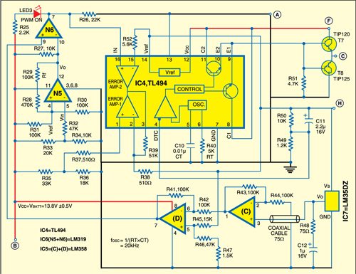
Fig. 5 shows the circuit of the PWM-based charge controller with main peripheral components. The over-current cum low-battery load-disconnect block whose output is to be connected to point D (and ground) and main charge-control PWM block whose output is to be connected to point C (and ground) are shown in separate figures (Figs 6 and 10, respectively) for the sake of clarity. Inputs/outputs to/from these two circuit blocks are connected to the circuit in Fig. 5 using circled points labeled ‘A’ through ‘G’. An emergency provision is made to bypass the control circuit (Fig. 6) and switch on the load directly by closing switch S1 in Fig. 5. However, bypassing the safety control circuit (Fig. 5) is not advisable under normal circumstances.
Over-load cum low-battery load-disconnect circuit. Fig. 6 shows the overload cum low-battery load-disconnect circuit. The output of this circuit is connected to point D in Fig. 5. As long as point D is at high voltage (> low-battery-voltage cut-off limit), n-channel MOSFET T4 (2N7000) will conduct to extend ground to the gate of p-channel MOSFET T2 (IRF9530). Thus MOSFET T2 also conducts and the battery/PV-module output is connected to the load. LED1 connected across the load through a 2.2-kilo-ohm resistor lights up to indicate that the load is ‘on.’
To prolong the battery life, there is a pro-vision to activate this circuit only when the load is switched on with the help of a push switch S2. It would remain ‘on’ until a low-battery condition or overload is detected by this circuit. Alternatively, to keep the circuit active all the time, the battery can be permanently connected to the circuit using a shorting link (JS). With this arrangement, the load will automatically switch on/off in accordance with the set points (refer Fig. 2). Additionally, manual switching on/off arrangements have been incorporated. The detailed description of the circuit (Fig. 6) follows.
This circuit uses a low-current (100mA) 5V regulator (78L05), a single-supply dual op-amp (LM358) and a quad comparator (LM339), apart from a few passive/active components as shown in Fig. 6. Assuming that presently over-current or low-battery conditions do not exist, the load should be ‘on’ if JS link is closed.
If JS is open and the load is not ‘on,’ regulator 78L05 connected across the load terminal (point G in Fig. 5) via 1N4007 diode will not activate and the remainder of the circuit too will not function and output D will be in high-impedance state. Pressing switch S2 momentarily applies battery voltage from point E to the regulator input as well as the remainder of the circuit via a 100μF capacitor for a brief period, causing point D to go high. As a result, it connects the battery to the load by activating the complementary pair of MOSFETs T2 and T4. Thereafter, the circuit remains latched in this state unless over-current or low-battery conditions are encountered. This will become clear to you once you go through further description of the circuit that follows.
In the circuit, op-amp LM358(A) is connected as a high-side current monitor. The differential input for this op-amp is the sense voltage (VSense=ILoad×RSense) developed across the 0.05-ohm resistor (RSense), which is connected across points B and E in Fig. 5. Out-put voltage Vo developed across resistor RB is given by the relationship:
Vo = VSense × RB/RA
(In the circuit, RA = 1 kilo-ohm and RB = 8.2 kilo-ohms)
If we assume the maxi-mum permissible load current as 8A, then:
VSense = 8x0.05V= 0.4V and Vo = 0.4x8.2 = 3.28V
Thus if you want the load to trip when current exceeds 8A, you should set the inverting pin of LM358(B) (connected as Schmitt trigger) at 3.28V. When the output voltage across RB (connected to its non-inverting pin) exceeds 3.28V, a positive pulse is generated at its output. This positive pulse sets comparator N1 (connected as a bistable) to high output state. (Note that N1 is initially reset to low output state because of slightly positive bias applied at its inverting pin with the help of resistive voltage divider formed by resistors R15 and R16). The high output of N1 is inverted by gate N2. Irrespective of the output state of comparator N2, point D is pulled low to switch off the load. Thus once overload occurs, the battery is disconnected from the load.

very useful article for both student and electronics professional.