


Includes a global shutter function and high effective pixel count for delivering high-quality, high-speed imaging performance
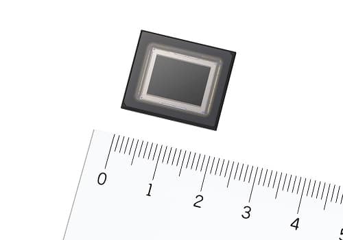

Thanks to components specialised for the UV wavelength, it is now possible to deliver a high level of UV sensitivity and high-quality imaging with minimal noise with the IMX487, a 2/3-type CMOS image sensor from Sony Semiconductor Solutions Corporation (Sony). The device is compatible with the UV (ultraviolet light) wavelength and comes with global shutter functionality, having a high effective pixel count of approximately 8.13 megapixels.
By utilising a unique back-illuminated pixel structure on a stacked CMOS image sensor, distortion-free imaging and high-speed performance are ensured. A compact form factor and high resolution give the industry’s smallest 2.74 µm square pixel size. The new sensor is useful in a variety of applications, including semiconductor pattern defect inspection in the existing UV camera market, thereby contributing to improving productivity in manufacturing processes and solving industrial issues. In general, UV cameras enable the sorting of materials that would be difficult in visible light, as well as checking for minute scratches and defects on the surface of objects.

This product employs material with a high level of UV transmittance for the optical path components that allows light to enter the product, in addition to a unique light receiving unit structure, ensuring high UV sensitivity and enabling high-quality imaging with significantly reduced noise. Additionally, the pixels capture UV light with high efficiency, resulting in high UV sensitivity as well as a tiny 2.74 µm square pixel size, which helps achieve the industry’s highest effective pixel count of approximately 8.13 megapixels even on a compact 2/3-type format.
The global shutter functionality enables distortion-free imaging of moving subjects and delivers high-speed performance at 193 frames per second (in 10-bit mode), thanks to the high degree of freedom of the wiring layout made possible by the back-illuminated pixel structure.
In addition to conventional UV image sensor applications such as semiconductor pattern defect inspection, the new product can be used to solve a variety of industrial challenges, including sorting plastics and other materials using UV light at recycling plants, inspecting for the application of transparent resin, inspecting for minute scratches on the surface of components, and detecting UV light emitted due to discharges in deteriorating overhead power lines.
Main Features
- Industry’s highest effective pixel count of approx. 8.13 megapixels, together with superb UV sensitivity and reduced noise
In addition to employing material with a high level of UV transmittance for the glass of the image sensor upper section and the pixel on-chip lenses, a unique structure specialised for UV is employed for the structure around the photodiode to deliver high UV sensitivity while ensuring high-quality imaging with reduced noise. Also, the pixels capture UV light with high efficiency, resulting in high UV sensitivity as well as a tiny 2.74 µm square pixel size, which helps achieve the industry’s highest effective pixel count of approximately 8.13 megapixels even on a compact 2/3-type format.
The compact form factor and high image quality not only makes this product suited to production line inspection applications but also makes it useful for addressing other challenges in applications such as outdoor infrastructure inspections, where portability and high resolution are required.
- Distortion-free high imaging performance and high-speed thanks to global shutter function with back-illuminated pixel structure
Sony’s Pregius S global shutter technology employs a unique back-illuminated pixel structure on a stacked CMOS image sensor, making it possible to deliver distortion-free moving subject imaging. Also, the high degree of freedom of the wiring layout afforded by the back-illuminated pixel structure enables high-speed performance at 193 frames per second (in 10-bit mode) for an image sensor compatible with the UV wavelength. This feature makes possible a range of applications where high-speed performance is required, including, for example, sorting plastics at a recycling plant using the UV wavelength.
