





A flip-flop (or a flip flop) is a digital circuit that stores just one bit of information, limited to either 0 or 1. Its output then depends on its inputs and the value it already holds. This ability to remember a state makes flip-flops essential building blocks for registers, counters and control circuits.
The four commonly taught types are SR, JK, D and T flip-flops. How do they differ? It is based on how their inputs determine the next stored value.
In this guide, “flip-flop” means an edge-triggered storage element. A latch is a related circuit that responds differently to its control signal.
Why is it called a Flip Flop in the first place?
Its name comes from its ability to “flip” or “flop” between two stable states. By latching a value and changing it when triggered by a clock signal, flip-flops can store data over time. Another way to put it, is that they are called flip-flops because they have two stable states and switch between them based on a triggering event.
It is the basic storage element in sequential logic. Next, let us clarify the difference between a latch and flip-flops in electronics.
Types of Flip-Flops at a Glance
| Type | Data inputs | What it does at the active clock edge | Typical use |
|---|---|---|---|
| SR Flip Flop | S and R | Sets, resets or holds the stored bit; one input combination is forbidden | Understanding set/reset storage and sequential logic |
| JK Flip Flop | J and K | Sets, resets, holds or toggles the stored bit | Counters and control circuits |
| D Flip Flop | D | Stores the value present at D | Registers, shift registers and state storage |
| T Flip Flop | T | Holds when T=0 and toggles when T=1 | Counters and frequency division |
The clock is separate from these data inputs. Some physical devices also have asynchronous preset and clear inputs.
How to Read the Truth Tables
The tables and equations below use:
- Q(t): the present stored value.
- Q(t+1): the next stored value.
- Q̅(t): the complement of Q(t).
- X: either 0 or 1, meaning “don’t care.”
An overbar means NOT, a dot means AND, a plus sign means OR, and ⊕ means XOR.
Unless stated otherwise, the tables describe behavior at the active clock edge, with asynchronous preset and clear inactive and timing requirements satisfied. Between active edges, the flip-flop holds its value.
1. SR Flip-Flop: Set and Reset
An SR flip-flop has two data inputs:
- S, which sets Q to 1.
- R, which resets Q to 0.
For the active-high convention used here, S=R=0 preserves the stored value. S=R=1 is forbidden because it requests set and reset simultaneously.
SR Flip-Flop Truth Table
| S | R | Q(t+1) | Operation |
|---|---|---|---|
| 0 | 0 | Q(t) | Hold |
| 0 | 1 | 0 | Reset |
| 1 | 0 | 1 | Set |
| 1 | 1 | Invalid | Forbidden input combination |
For valid inputs, its characteristic equation is:
Q(t+1) = S + R̅ · Q(t)
The condition S · R = 0 must be maintained.
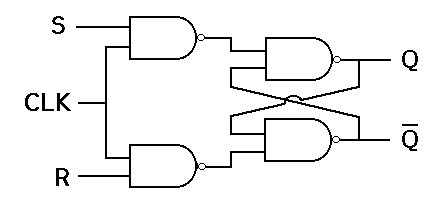
SR Latch Circuit and Input Conventions
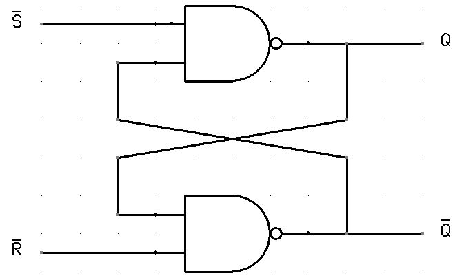
Two cross-coupled NOR gates form a basic active-high SR latch. Two cross-coupled NAND gates form an active-low SR latch, usually labelled with inputs S̅ and R̅.
Their input conventions differ:
| Circuit | Hold condition | Forbidden condition |
|---|---|---|
| NOR SR latch, active-high inputs | S=R=0 | S=R=1 |
| NAND SR latch, active-low inputs | S̅=R̅=1 | S̅=R̅=0 |
These cross-coupled circuits are latches. Adding an enable signal produces a gated latch; edge-triggered operation requires an appropriate additional circuit arrangement. Reference: University of California, Riverside
Read more about SR flip-flop operation, limitations and applications.
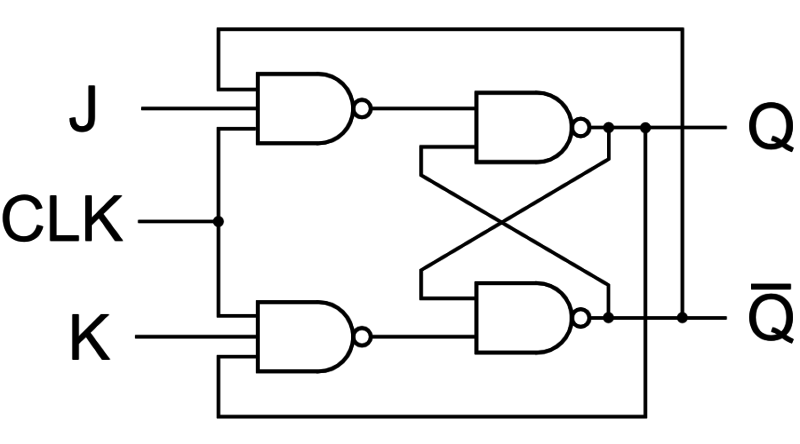
2. JK Flip-Flop: Set, Reset, Hold and Toggle
A JK flip-flop provides four operating modes. Its J input performs the set function, while K performs the reset function.
When both inputs are 1, the output toggles: a stored 0 becomes 1, and a stored 1 becomes 0.
JK Flip-Flop Truth Table
| J | K | Q(t+1) | Operation |
|---|---|---|---|
| 0 | 0 | Q(t) | Hold |
| 0 | 1 | 0 | Reset |
| 1 | 0 | 1 | Set |
| 1 | 1 | Q̅(t) | Toggle |
Its characteristic equation is:
Q(t+1) = J · Q̅(t) + K̅ · Q(t)
For example, if Q(t)=0 and J=K=1, the next active clock edge changes Q to 1. Keeping J=K=1 makes the following active edge change Q back to 0.
What Is the Race-Around Condition?
In a level-sensitive JK implementation with feedback, J=K=1 can cause repeated toggling while the clock remains active. If the active interval permits multiple transitions, the final state may be unpredictable.
An appropriate edge-triggered or master-slave implementation prevents this repeated feedback-driven toggling during one clock pulse. Device timing requirements still apply. Reference: Georgia State University
Read more about JK flip-flop circuits and applications.
3. D Flip-Flop: Store the Input Data
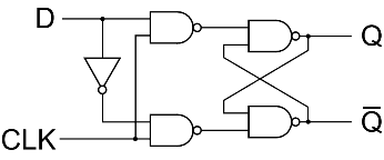
A D flip-flop has one data input, D. At its active clock edge, it stores the value at that input:
Q(t+1) = D
The D input can change between clock edges without immediately changing Q.
D Flip-Flop Truth Table
For a positive-edge-triggered D flip-flop:
| Clock event | D | Q(t+1) | Operation |
|---|---|---|---|
| Rising edge ↑ | 0 | 0 | Store 0 |
| Rising edge ↑ | 1 | 1 | Store 1 |
| No rising edge | X | Q(t) | Hold |
A negative-edge-triggered version captures D on the falling edge instead.
Example: Following a Data Sequence
Suppose D has the values 1, 0, 1, 1 at four successive rising clock edges. Q stores the same sequence after those edges, allowing for the device’s propagation delay.
A short pulse on D entirely between rising edges is not captured if it does not overlap the sampling interval.
D flip-flops are widely used in registers and shift registers. For a physical example, the SN74HC74 contains two positive-edge-triggered D flip-flops with asynchronous preset and clear inputs. Reference: Texas Instruments
Read more about D flip-flop operation and applications.
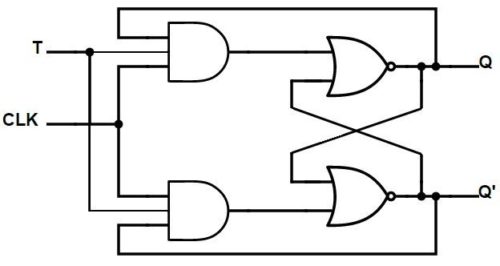
4. T Flip-Flop: Toggle the Stored Value
The T input determines whether a T flip-flop holds or changes its state:
- T=0: hold the present value.
- T=1: toggle at the active clock edge.
T Flip-Flop Truth Table
| T | Q(t) | Q(t+1) | Operation |
|---|---|---|---|
| 0 | 0 | 0 | Hold |
| 0 | 1 | 1 | Hold |
| 1 | 0 | 1 | Toggle |
| 1 | 1 | 0 | Toggle |
Its characteristic equation is:
Q(t+1) = T ⊕ Q(t)
How to Make a T Flip-Flop
Two common implementations are:
- Using a JK flip-flop: connect J and K together and drive both with T.
- Using a D flip-flop: feed D from an XOR gate whose inputs are T and Q.
The second implementation uses D = T ⊕ Q. Connecting Q̅ directly to D creates a circuit that toggles on every active edge, equivalent to holding T at 1. Reference: Iowa State University
Read more about T flip-flop circuits and uses.
Flip-Flop vs Latch: What Is the Difference?
The main difference is when the stored value can change.
| Feature | Latch | Edge-triggered flip-flop |
|---|---|---|
| Response to control signal | Level-sensitive | Edge-sensitive |
| When data can affect the output | While the latch is enabled | At the active clock edge |
| Between updates | Holds when disabled | Holds between active edges |
| Basic example | Gated D latch | Positive-edge-triggered D flip-flop |
A D latch is transparent while enabled: changes at D can pass through to Q. A D flip-flop samples D around a clock transition and holds that value until the next active transition. Asynchronous controls, where present, can override normal clocked operation. Reference: Northwestern University
See our detailed guide to the difference between latches and flip-flops.
A flip-flop is a synchronous Circuit and is also known as a gated or clocked SR latch. In this circuit diagram, the output is changed (i.e. the stored data is changed) only when you give an active clock signal. Otherwise, even if the S or R is active, the data will not change.
What Device is a Flip-flop? A flip-flop is not a specific device but rather a term used to describe a group of sequential logic circuits. These circuits made up of digital logic gates and other components, can be created using different electronic elements like transistors, integrated circuits (ICs), or programmable logic devices (PLDs).
Let’s understand the flip-flop in detail with the truth table and circuits.
Clock Edges and Timing Requirements
A rising edge is a clock transition from 0 to 1. A falling edge is a transition from 1 to 0. The device’s symbol and datasheet specify which transition triggers it. Reference: Duke University
Real flip-flops also have timing requirements:
| Timing term | Meaning |
|---|---|
| Setup time | Minimum time the data must remain stable before the active edge |
| Hold time | Minimum time the data must remain stable after the active edge |
| Clock-to-Q delay | Time from the active edge to the resulting output change |
Violating setup or hold requirements can produce an incorrect capture or metastability, where the output takes longer than expected to settle.
For a single-bit signal arriving from another clock domain, designers commonly use a synchronizer consisting of two or more flip-flop stages. This reduces the probability of metastability reaching downstream logic. Multi-bit transfers require additional coordination.
Characteristic Tables vs Excitation Tables
A characteristic table answers:
Given the current state and inputs, what will the next state be?
An excitation table answers:
Given the current state and required next state, which inputs are needed?
Combined Flip-Flop Excitation Table
| Q(t) | Required Q(t+1) | SR inputs (S, R) | JK inputs (J, K) | D | T |
|---|---|---|---|---|---|
| 0 | 0 | 0, X | 0, X | 0 | 0 |
| 0 | 1 | 1, 0 | 1, X | 1 | 1 |
| 1 | 0 | 0, 1 | X, 1 | 0 | 1 |
| 1 | 1 | X, 0 | X, 0 | 1 | 0 |
Here, X means either input value produces the required transition under the stated conditions. It does not mean the output is unknown.
Excitation tables are useful when designing counters, state machines and flip-flop conversions. Reference: University of Florida
Flip Flop Conversion
Flip-flop conversion refers to the process of modifying one type of flip-flop (e.g., SR, D, JK, or T) to behave like another type by designing an appropriate input logic circuit. This is often required when a specific flip-flop is not directly available or for simplifying circuit design.
The method is to:
- Write the required next-state behavior.
- Identify the inputs the available flip-flop needs for each transition.
- Simplify the input expressions.
- Connect the required logic gates.
- Check every valid input and current-state combination.
Common Flip-Flop Conversion Equations
In this table, Q is the available flip-flop’s present output.
| Available type | Required behavior | Connect the available inputs as follows |
|---|---|---|
| SR | D | S=D; R=D̅ |
| SR | JK | S=J · Q̅; R=K · Q |
| SR | T | S=T · Q̅; R=T · Q |
| JK | SR | J=S; K=R; exclude S=R=1 |
| JK | D | J=D; K=D̅ |
| JK | T | J=T; K=T |
| D | SR | D=S + R̅ · Q; exclude S=R=1 |
| D | JK | D=J · Q̅ + K̅ · Q |
| D | T | D=T ⊕ Q |
These equations describe valid synchronous next-state behavior. They assume compatible clocking and inactive asynchronous controls. Applying the same feedback connections to a transparent latch does not automatically produce an edge-triggered flip-flop.
Worked Example: Convert a D Flip-Flop to T
A D flip-flop stores whatever appears at D. To reproduce T behavior, D must equal:
- Q when T=0, so the state is held.
- Q̅ when T=1, so the state changes.
An XOR gate provides exactly this function:
D = T ⊕ Q
For T=1 and Q=0, the gate produces D=1. The next active edge stores 1. After Q changes, the gate produces D=0, ready for the following active edge.
Applications of Flip-Flops
Registers
A register groups flip-flops to store a binary word. Eight D flip-flops can store an 8-bit value, with each flip-flop holding one bit.
Shift Registers
Connecting one stage’s Q output to the next stage’s D input allows data to move through the register on successive clock edges. Shift registers support serial-to-parallel and parallel-to-serial conversion.
Counters
Flip-flops store a counter’s binary state. T and JK flip-flops provide convenient toggle behavior, while D flip-flops can implement counters using next-state logic.
Frequency Dividers
A flip-flop that toggles on every active clock edge completes one output cycle for every two input cycles:
Output frequency = Input frequency ÷ 2
Control Circuits
Flip-flops store the state of a sequential controller. Input logic determines when the controller should move to its next state.
Input Synchronization
Flip-flop chains help transfer suitable single-bit signals into a receiving clock domain, reducing the chance that metastability affects the rest of the circuit.
Practical Circuit Example: Divide a Clock by Two
A D flip-flop can act as a frequency divider by feeding its inverted output back to its data input.
Using one section of an SN74HC74:
- Connect Q̅ to D.
- Apply a compatible clock signal to CLK.
- Keep the active-low preset and clear inputs inactive during normal counting.
- Take the divided clock from Q.
At each rising edge, the flip-flop captures the opposite of its current value. A 1 kHz input therefore produces a nominal 500 Hz output.
Use clear to establish a known initial state when required, and follow the datasheet’s power, input and timing requirements. Reference: Texas Instruments SN74HC74 datasheet
General Steps for Flip-Flop Conversion
- Understand the Source and Target Flip-Flops:
- Identify the type of flip-flop you have (source flip-flop) and the type you want to convert it into (target flip-flop).
- Know the characteristic equations and truth tables for both types.
- Write the Truth Table for the Target Flip-Flop:
- Create a truth table for the target flip-flop based on its characteristic equation and behaviour. Include the current state (Q), the input of the target flip-flop, and the next state (Qnext).
- Relate the Target and Source Flip-Flops:
- For each possible combination of Q (current state) and Qnext (desired next state), determine the required inputs for the source flip-flop to achieve the same behaviour.
- Determine the Input Expressions:
- Derive the logic expressions for the inputs of the source flip-flop that will allow it to produce the same output transitions as the target flip-flop.
- Use Karnaugh maps (K-maps) or Boolean algebra to simplify the input logic expressions.
- Design the Conversion Logic Circuit:
- Use the simplified expressions to design a circuit using logic gates that connect the input(s) of the source flip-flop to behave like the target flip-flop.
- Verify the Conversion:
- Validate the conversion by ensuring that the source flip-flop with the designed logic produces the same Qnext as the target flip-flop for all input conditions.
SR Flip-Flop Conversion to Other Flip-Flops
Converting SR Flip-Flop to JK Flip-Flop
To convert an SR flip-flop into a JK flip-flop, we need to design a combinational circuit with J and K as inputs, which are then connected to the SR flip-flop inputs. The goal is for the output to mimic the behaviour of a JK flip-flop.
Here’s the process:
- Start by creating a truth table for J, K, and the present state (QP), considering all possible combinations.
- For each combination, determine the next state (QN).
- Identify the S and R values needed to transition from QP to QN.
Using the truth table, the Boolean equations for S and R are derived using Karnaugh maps:
The logic diagram for the JK flip-flop implemented from an SR flip-flop connects these inputs through the derived equations.

Converting SR Flip-Flop to D Flip-Flop
Transforming an SR flip-flop into a D flip-flop is simpler. The Data (D) input is connected to the S input, while its inverted form (D’) is connected to the R input. The Boolean equations derived from the truth table are:
- S=D
- R=D’
This setup ensures the SR flip-flop behaves like a D flip-flop, storing the input data in sync with the clock signal.

Converting SR Flip-Flop to T Flip-Flop
To convert an SR flip-flop to a T flip-flop, a combinational circuit is designed using the Toggle (T) input and the present state (QP).
- Truth tables are used to determine the required S and R values for each T and QP combination.
- The derived equations are:
The resulting circuit enables toggling the state of the flip-flop based on the T input.
JK Flip-Flop Conversion
Converting JK Flip-Flop to SR Flip-Flop
The JK flip-flop can be directly converted into an SR flip-flop because the logic for J and K aligns with S and R.
- J=S
- K=R
No additional circuitry is needed—simply relabel the inputs.

Converting JK Flip-Flop to D Flip-Flop
To transform a JK flip-flop into a D flip-flop:
- The Data (D) input connects directly to J.
- The inverted D (D’) connects to K.
The Boolean equations are straightforward:
- J=D
- K=D’
This ensures the JK flip-flop stores and outputs the D input correctly.

Converting JK Flip-Flop to T Flip-Flop
Converting a JK flip-flop into a T flip-flop is as simple as connecting the T input directly to both J and K.
- J=T
- K=T
This enables toggling functionality with minimal changes.

D Flip-Flop Conversion
Converting D Flip-Flop to SR Flip-Flop
To convert a D flip-flop to an SR flip-flop, a combinational circuit is added to derive S and R from D.
- Truth tables show:
- S=D
- R=D’
This design aligns the D flip-flop to behave like an SR flip-flop.

Converting D Flip-Flop to JK Flip-Flop
The conversion involves creating J and K inputs based on the D input.
- J=D
- K=D’
These connections ensure the D flip-flop functions as a JK flip-flop.

Converting D Flip-Flop to T Flip-Flop
A D flip-flop can also function as a T flip-flop by using the T input to toggle the state. No additional combinational logic is required for this simple conversion.
FAQs
What is a flip-flop in digital electronics?
A flip-flop is a sequential logic circuit that stores one bit, either 0 or 1. An edge-triggered flip-flop updates its stored value at a specified clock transition, unless an asynchronous control overrides it.
What are the four main types of flip-flops?
The four commonly taught types are SR, JK, D and T. SR provides set and reset functions, JK adds toggle behavior, D stores its data input, and T holds or toggles the stored value.
Why is it called a flip-flop?
The name describes its ability to switch between two stable states. These states represent binary 0 and binary 1.
Are SR and RS flip-flops the same?
SR and RS usually refer to the same set/reset function, with the letters written in a different order. Always check the circuit’s input labels, active levels and truth table.
What happens when both SR inputs are 1?
For an active-high SR device, S=R=1 is forbidden. In a basic NOR SR latch, this condition forces both outputs low while asserted, and simultaneous release can leave the final stored state uncertain. An active-low NAND latch has a different forbidden combination: both inputs low.
What happens when J and K are both 1?
An edge-triggered JK flip-flop toggles at its active clock edge. If Q was 0, it becomes 1. If Q was 1, it becomes 0, assuming normal timing and inactive asynchronous controls.
Does a D flip-flop change whenever D changes?
No. In normal operation, an edge-triggered D flip-flop captures D at its active clock edge. Changes between active edges do not immediately change its output.
Is a master-slave flip-flop the same as an SR flip-flop?
No. “SR” describes the input behavior. “Master-slave” describes an internal arrangement using two storage stages controlled in different clock phases. It is an implementation approach rather than another name for SR.
Which flip-flop is used in counters?
Counters can use T, JK or D flip-flops. T and JK types offer toggle behavior directly. D flip-flops use additional logic to calculate the next count.
How many flip-flops are needed to store eight bits?
Eight one-bit flip-flops are needed to store eight bits. Additional circuitry may provide functions such as loading, resetting or shifting the data.
Do flip-flops retain data when power is removed?
Ordinary flip-flops are volatile and do not retain their stored data after power is removed. A circuit that needs to preserve information without power requires nonvolatile storage or another retention mechanism.
How is a flip-flop different from a logic gate?
A combinational logic gate produces an output from its current inputs. A flip-flop also stores a state, so its behavior depends on previously stored information. This is what makes it part of sequential logic.
We hope this article helped you understand Flip-Flops in digital electronics.
If you have any doubts, please feel free to ask in the comments section below.
This article was first published on 17 August 2017 and updated in 22 September 2026.

simple for me to understand good
i think the diagram for SR – flip flop is wrong dude.
No bro
Yeah, the AND gates are supposed to be OR gates. Funny huh
you are wong
they are suppose to be or gates. you are wrong
He is right and so are you. There’s 2 ways to make an S-R latch.
The most common one is using AND gates followed my NOR gates.
The second way is using only NAND gates like he is using above.
the only difference is when we activate S and R at the same time (which is to be avoided)
hi
Shouldn’t the second row second column element of Truth table for T-flip flop be ‘0’ instead of ‘1’? i.e., when T = 1 and Q = 0 the output is 1.
good
well explained
Thank you for your feedback.
your second row of t flip flop is wrong please correct it many student refer your site . So rectify as soon as possible .
Exactly it’s a rs flip flop
what is the correction dude?
Excellent
Hi, I would like to construct a single touch switch using a D flip flop IC, 555 timer, 5v relay module and a capacitive touch pad. So how do i connect the D flip flop to the touch switch circuit for it to work. please i need a reply.
This article needs correction. A D-latch isn’t the same thing as a D Flip flop
It’s good
Thank You for your feedback.
Anyone please clarify what does the author mean by the jargon ‘clock edge’. What does he mean exactly?
Can you give this JK flip flop IC implementation?